Making Semiconductor Devices with Alignment Bonding and Substrate Removal

a technology of alignment bonding and substrate removal, applied in the direction of semiconductor devices, basic electric elements, electrical equipment, etc., can solve the problems of limited battery operation time, low light efficiency, and high power consumption

Active Publication Date: 2017-06-22
JADE BIRD DISPLAY SHANG HAI LTD
View PDF2 Cites 108 Cited by
  • Summary
  • Abstract
  • Description
  • Claims
  • Application Information

AI Technical Summary

Problems solved by technology

However, conventional LCD displays suffer from low light efficiency, causing high power consumption and limited battery operation time.
However, the integration of thousands or even millions of micro LEDs with pixel driver circuit array is quite challenging.
However, this fabrication process is inefficient and costly.
In addition, there are no existing manufacturing tools for mass transferring micro LEDs.
The substrate on which the LEDs are fabricated remains in the final product, which may cause light cross-talk.
Additionally, the thermal mismatch between the two different substrates generates stress at the bonding interface, which can cause reliability issues.
Furthermore, multi-color display panels typically require more LEDs and different color LEDs grown on different substrate materials, compared with single-color display panels, thus making the traditional manufacturing process even more complicated and inefficient.

Method used


Image

  • Making Semiconductor Devices with Alignment Bonding and Substrate Removal
  • Making Semiconductor Devices with Alignment Bonding and Substrate Removal
  • Making Semiconductor Devices with Alignment Bonding and Substrate Removal

Examples


Embodiment Construction

[0024]The figures and the following description relate to preferred embodiments by way of illustration only. It should be noted that from the following discussion, alternative embodiments of the structures and methods disclosed herein will be readily recognized as viable alternatives that may be employed without departing from the principles of what is claimed.

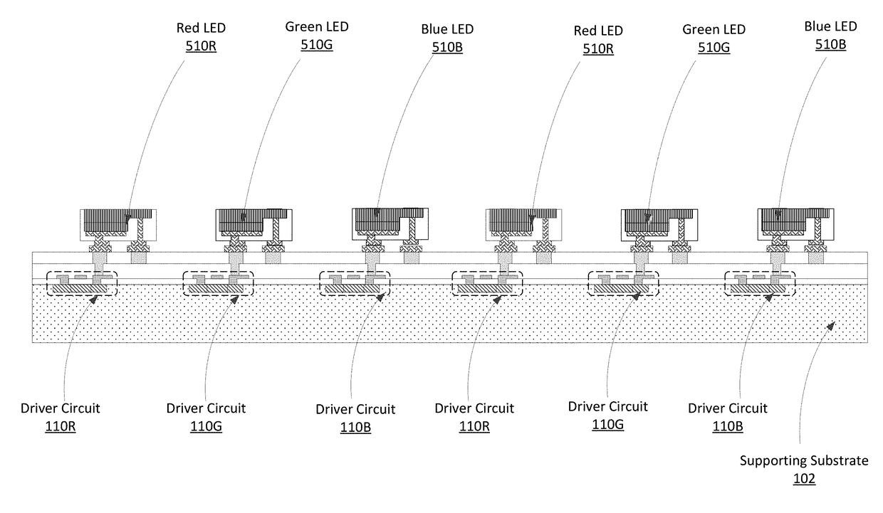
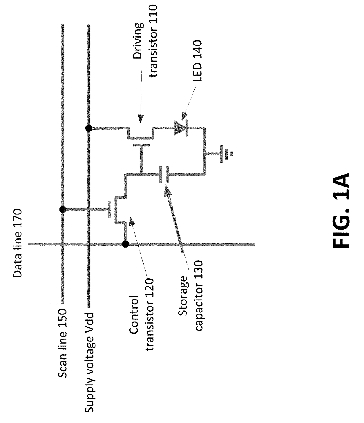
[0025]FIG. 1A is a circuit diagram of a pixel of a display panel, which includes a pixel driver and LED 140. In this example, the pixel driver includes two transistors and one capacitor 130, with one transistor being a control transistor 120 and the other being a driving transistor 110. In this example, the control transistor 120 is configured with its gate connected to a scan signal bus line 150, its one source / drain connected to a data signal bus line 170, and the other drain / source connected to the storage capacitor 130 and to the gate of the driving transistor 110. One source / drain of the driving transistor 110 is connecte...


PUM


Abstract

Embodiments include a manufacturing method of making a semiconductor device via multiple stages of alignment bonding and substrate removal. One example is an integrated full-color LED display panel, in which multiple wafers with different arrays of LEDs are integrated onto a host wafer with driver circuitry. The driver circuitry typically is an array of pixel drivers that drive individual LEDs on the display panel.

Description

CROSS-REFERENCE TO RELATED APPLICATION(S)[0001]This application claims priority under 35 U.S.C. §119(e) to U.S. Provisional Patent Application Ser. No. 62 / 270,376, entitled “Method of Making RGB LED Micro-Display by Multiple Alignment Bonding and Substrate Removal Process,” filed on Dec. 21, 2015. The subject matter of all of the foregoing is incorporated herein by reference in their entirety.BACKGROUND[0002]1. Field of the Invention[0003]This disclosure relates generally to methods for fabricating semiconductor devices, for example, methods for fabricating integrated multi-color LED display panels.[0004]2. Description of Related Art[0005]Active matrix liquid-crystal displays (LCD) and organic light emitting diode (OLED) displays combined with thin-film transistor (TFT) technology are becoming increasingly popular in today's commercial electronic devices. These displays are widely used in laptop personal computers, smartphones and personal digital assistants. Millions of pixels toge...

Claims


Application Information

Patent Timeline
Patent Type & Authority Applications(United States)
IPC IPC(8): H01L25/00H01L25/16H01L27/12H01L27/15
CPCH01L25/50H01L27/156H01L27/124H01L27/1262H01L25/167H01L25/0753H01L33/62H01L33/0093
Inventor ZHANG, LEIOU, FANGLI, QIMING
Owner JADE BIRD DISPLAY SHANG HAI LTD
Why Eureka
Try Eureka