Transistor array panel and manufacturing method thereof

a technology of transistor array panel and manufacturing method, which is applied in the direction of transistors, electrical devices, semiconductor devices, etc., can solve the problems of low charge mobility, high product cost, and complicated manufacturing process, and achieve the effect of improving the quality reducing the number of processing stages used for manufacturing a transistor array panel, and improving the properties of the transistor array panel

Active Publication Date: 2017-06-22
SAMSUNG DISPLAY CO LTD
View PDF15 Cites 5 Cited by
  • Summary
  • Abstract
  • Description
  • Claims
  • Application Information

AI Technical Summary

Benefits of technology

[0029]According to the exemplary embodiments of the present disclosure, the transistor properties, such as output saturation, can be improved. Further, the number of masks and processing stages used for manufacturing a transistor array panel can be reduced, and quality of the transistor array panel can be improved.

Problems solved by technology

Amorphous silicon has a simple manufacturing process but a low charge mobility, so is rarely used in high-performance transistors, while polysilicon has high charge mobility but requires a process for crystallizing the silicon, so its product cost is high and its manufacturing process is complicated.

Method used


Image

  • Transistor array panel and manufacturing method thereof
  • Transistor array panel and manufacturing method thereof
  • Transistor array panel and manufacturing method thereof

Examples


Embodiment Construction

[0035]In the following detailed description, only certain exemplary embodiments of the present disclosure have been shown and described, simply by way of illustration. As those skilled in the art would realize, the described embodiments may be modified in various different ways, all without departing from the spirit or scope of the present disclosure.

[0036]Like reference numerals may designate like elements throughout the specification. In the drawings, the thickness or sizes of respective layers and regions may be enlarged or reduced to clearly illustrate their arrangements and relative positions.

[0037]In the specification, it will be understood that when an element such as a layer, film, region, or substrate is referred to as being “on” another element, it can be directly on the other element or intervening elements may also be present.

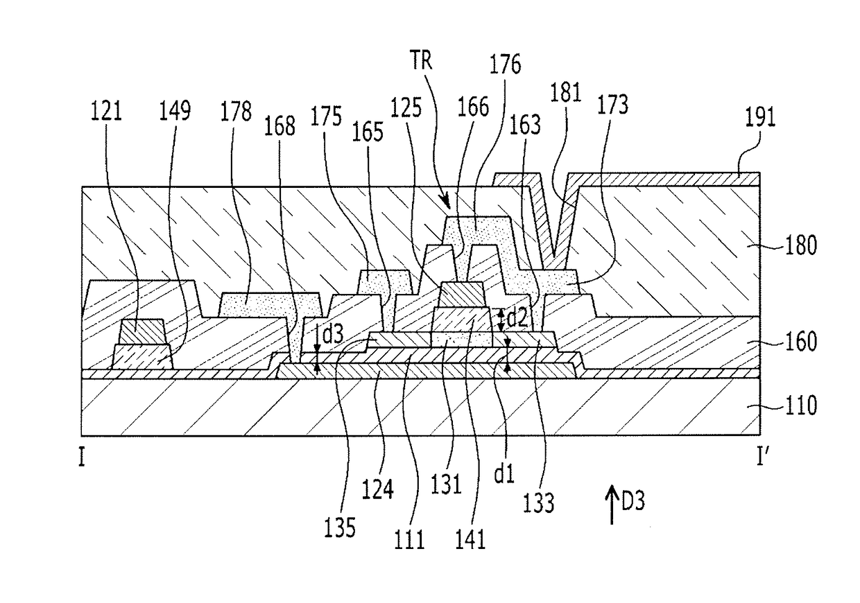
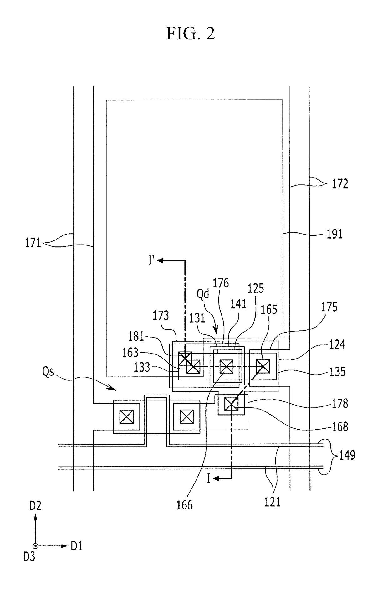
[0038]A transistor array panel according to an exemplary embodiment of the present disclosure will now be described with reference to accompanying ...


PUM


Abstract

A transistor array panel includes a transistor disposed on a substrate. The transistor includes a gate electrode, a source electrode, a drain electrode, a semiconductor, and a top electrode. The top electrode is disposed on and overlaps the semiconductor, and is electrically connected to the source electrode.

Description

CROSS-REFERENCE TO RELATED APPLICATION[0001]This application claims priority under 35 U.S.C. §119from, and the benefit of, Korean Patent Application No. 10-2015-0180450, filed in the Korean Intellectual Property Office on Dec. 16, 2015, the contents of which are herein incorporated by reference in their entirety.BACKGROUND[0002](a) Technical Field[0003]Embodiments of the present disclosure are directed to a transistor array panel and a manufacturing method thereof.[0004](b) Discussion of the Related Art[0005]Transistors are included in various electronic devices such as a display device, and include a gate electrode, a source electrode, a drain electrode, and a semiconductor. A transistor can be used as a switching element or a driving element for the display device.[0006]The semiconductor determines characteristics of the transistor. Silicon (Si) is generally used for the semiconductor. Silicon (Si) can be classified as amorphous silicon or polysilicon, depending on crystal pattern...

Claims


Application Information

Patent Timeline
Patent Type & Authority Applications(United States)
IPC IPC(8): H01L27/12H01L21/44H01L29/786H01L29/417H01L29/423
CPCH01L27/124H01L29/41733H01L27/1248H01L21/44H01L29/7869H01L27/1288H01L29/42384H01L29/78648H01L27/1225H10K59/1213
Inventor LEE, SANG KYUNGMOON, SANG-HO
Owner SAMSUNG DISPLAY CO LTD
Why Eureka
Try Eureka