Method of Designing Electroluminescent Device, Electroluminescent Device Manufactured with the Design Method, and Method of Manufacturing Electroluminescent Device with the Design Method

a technology of electroluminescent devices and design methods, which is applied in the direction of computer aided design, organic semiconductor devices, instruments, etc., can solve the problems of disadvantageous control of electroluminescent devices, and achieve accurate estimation

Active Publication Date: 2017-06-22
MERCK PATENT GMBH
View PDF1 Cites 4 Cited by
  • Summary
  • Abstract
  • Description
  • Claims
  • Application Information

AI Technical Summary

Benefits of technology

[0019]According to this method of manufacturing an electroluminescent device, a method of designing an electroluminescent device which allows more accurate computation of an external emission spectrum output to the outside in a current injection state and accurate estimation of a quantity and / or a color of light extracted to the outside, an electroluminescent device manufactured with the design method, and a method of manufacturing an electroluminescent device with the design method can be provided.

Problems solved by technology

A color or a luminance of light extracted to the outside, however, is varied due to interference with an optical multi-layer, and control thereof is disadvantageously difficult.

Method used


Image

  • Method of Designing Electroluminescent Device, Electroluminescent Device Manufactured with the Design Method, and Method of Manufacturing Electroluminescent Device with the Design Method
  • Method of Designing Electroluminescent Device, Electroluminescent Device Manufactured with the Design Method, and Method of Manufacturing Electroluminescent Device with the Design Method
  • Method of Designing Electroluminescent Device, Electroluminescent Device Manufactured with the Design Method, and Method of Manufacturing Electroluminescent Device with the Design Method

Examples


examples

[0213][5.1 Single-Emission Light-Emitting Device]

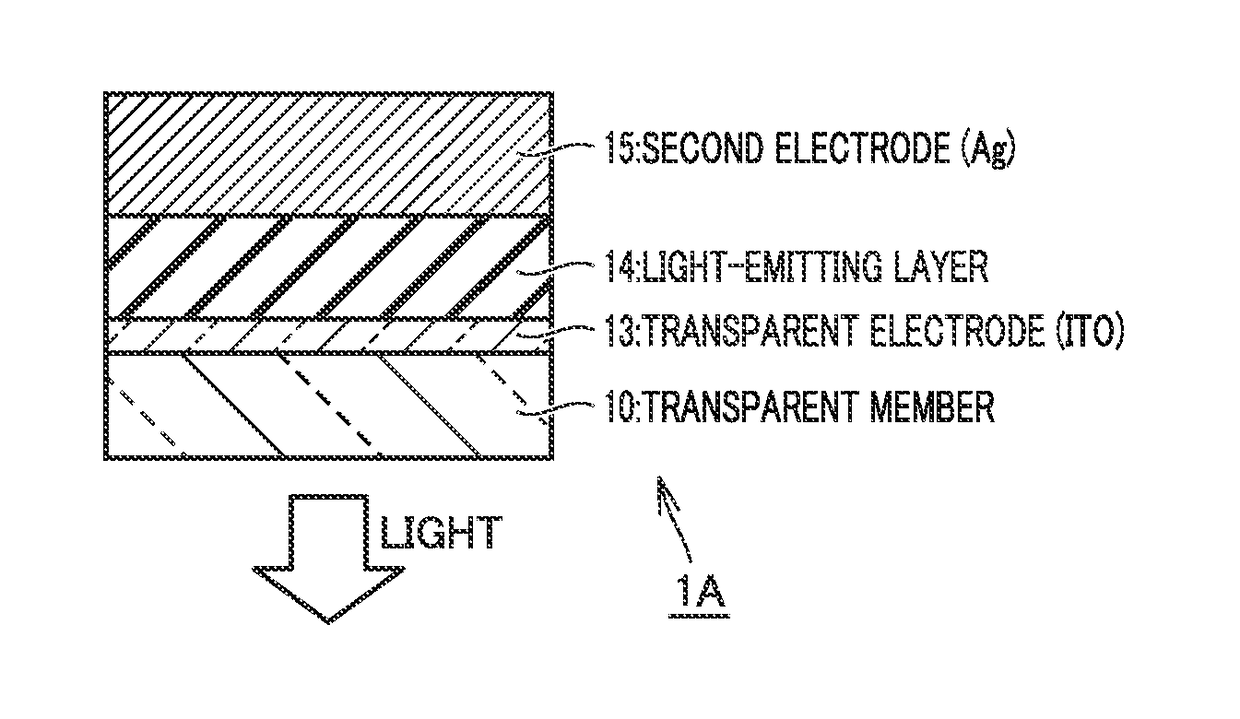
[0214]In order to describe the effect of the present embodiment in further detail, description will be given below with reference to analysis of an organic electroluminescent device. Organic EL electroluminescent device 100 to be analyzed has a structure shown in FIG. 22, in which ITO (having a thickness of 150 nm) was provided as transparent electrode 113 on a glass substrate as transparent member 110 and first functional layer 114a, emissive layer 114c (having a thickness of 20 nm), and second functional layer 114e were provided through vacuum vapor deposition. Thereafter, an Ag film (having a thickness of 100 nm) serving as a reflective electrode was provided as second electrode 15. A green phosphorescent material having an emission peak wavelength of 520 nm was employed for emissive layer 114c. First functional layer 114a was constituted of a hole injection layer, a hole transfer layer, and an electron blocking layer (a total of 3...


PUM


Abstract

A method of designing an electroluminescent device allows more accurate computation of an external emission spectrum output to the outside in a current injection state and accurate estimate of a quantity and / or a color of light extracted to the outside, an electroluminescent device manufactured with the design method, and a method of manufacturing an electroluminescent device with the design method.

Description

TECHNICAL FIELD[0001]The present invention relates to a method of designing an electroluminescent device, an electroluminescent device manufactured with the design method, and a method of manufacturing an electroluminescent device with the design method.BACKGROUND ART[0002]A surface emitting device high in luminous efficiency which includes an electroluminescent device such as a light-emitting diode (LED) or organic EL has recently attracted attention. The electroluminescent device is formed from an emissive layer lying between a planar cathode and a planar anode, and generally in many cases, it is formed from a transparent electrode as an anode and a metal reflective electrode as a cathode.[0003]When the cathode is formed from a metal electrode, light is extracted from a side of the transparent anode, and the electroluminescent device is used as a single-emission light emitting device. When electrodes on opposing sides are formed from transparent electrodes, a transparent light emi...

Claims


Application Information

Patent Timeline
Patent Type & Authority Applications(United States)
IPC IPC(8): H01L51/56G06F17/50H01L33/58H01L51/00H01L51/52H01L33/44
CPCH01L51/56H01L51/5268H01L51/5275H01L51/5265H01L33/44H01L33/58G06F2217/12G06F17/5081H01L2251/56H01L2251/558H01L2933/0091H01L2933/0058H01L2933/0025H01L51/0031H10K50/816H10K50/852H10K50/854H10K50/858H10K2102/3031H10K2102/3026H10K2102/351H10K71/00H05B33/10H10K71/70H10K50/00H10K50/828H10K50/85G06F30/398G06F2119/18
Inventor OSAWA, KOUSEKINE, KOUJIROUYOKOYAMA, MITSURU
Owner MERCK PATENT GMBH
Why Eureka
Try Eureka