Shape based grouping

a grouping and shape technology, applied in image analysis, image enhancement, instruments, etc., can solve the problems of increasing reducing the yield, and reducing the efficiency of the semiconductor manufacturing process, so as to achieve the effect of improving the quality of the semiconductor, reducing the cost of the process, and reducing the cost of the overall semiconductor manufacturing cos

Active Publication Date: 2017-06-29
KLA TENCOR TECH CORP
View PDF9 Cites 24 Cited by
  • Summary
  • Abstract
  • Description
  • Claims
  • Application Information

AI Technical Summary

Benefits of technology

[0017]In a first embodiment, a system is provided. The system comprises a review tool and a controller. The review tool includes a stage configured to hold a wafer and an image generation system configured to generate an image of the wafer. The controller is in electronic communication with the review tool. The controller is configured to: request design polygons in a field of view centered at one or more defect locations of the wafer; render a binary image showing the design polygons in the

Problems solved by technology

Defects cause wafer yields to decline, causing increases in overall semiconductor manufacturing costs.
The process of reviewing semiconductor defects in a semiconductor fabrication facility or foundry is expensive in terms of both human effort and time.
Review tools can produce resolved and high magnification images for a user, but review tools tend to be slow.
This classification process requires extensive human effort and is slow, which results in high operational costs.
By the quantitative nature of its language and coding mechanism, users have difficulty writing “rules” with DBG.
The defects arising at these locations can be rare but disastrous, and DBG based review sampling that relies solely on statistics may miss this tiny population if limits are set on the sample size.
This can create too many groups.
Hence, a sampling which relies on DBG groups may miss an important defect type, or it may sample too many of the same type.
These DBG deficiencies may not result in efficient review sampling.
Therefore, there can be thousands of such complex

Method used


Image

  • Shape based grouping
  • Shape based grouping
  • Shape based grouping

Examples


Embodiment Construction

[0047]Although claimed subject matter will be described in terms of certain embodiments, other embodiments, including embodiments that do not provide all of the benefits and features set forth herein, are also within the scope of this disclosure. Various structural, logical, process step, and electronic changes may be made without departing from the scope of the disclosure. Accordingly, the scope of the disclosure is defined only by reference to the appended claims.

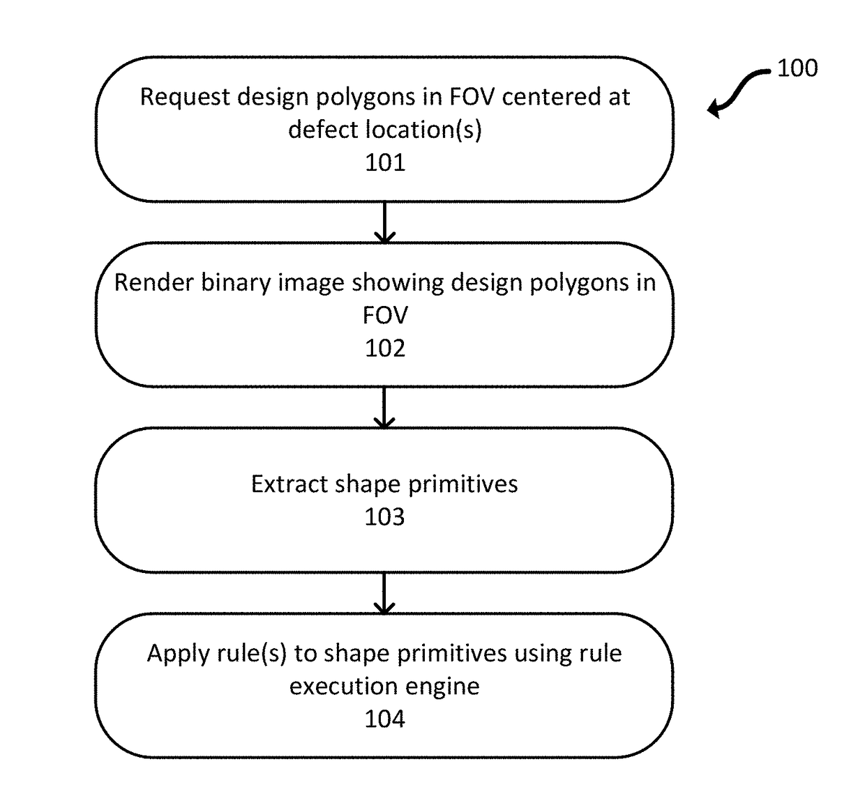
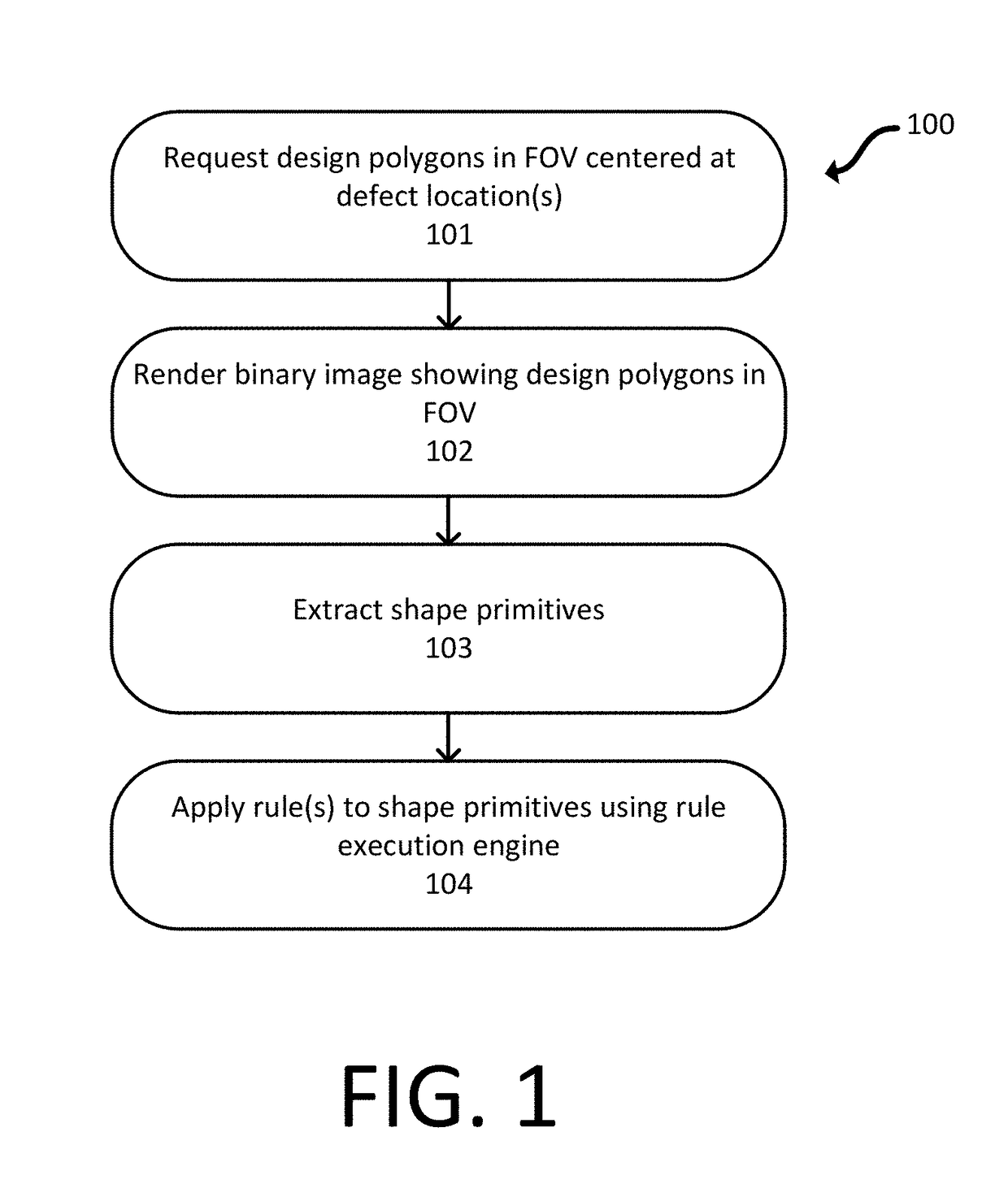
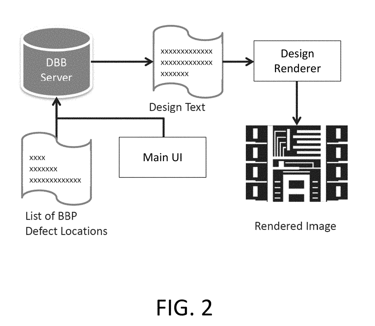
[0048]Shape based grouping (SBG) can improve the efficiency of the review sampling of systematic defects caused by failure prone local design patterns called “hotspots” on a semiconductor wafer in a fabrication facility or foundry through a succinct description of the local spatial relationships between the shapes in the design describing the local circuit pattern on the wafer layer(s), possibly coupled with the corresponding image data from an inspection or review tool. The defects at these locations are assumed to be ca...


PUM


Abstract

Shape primitives are used for inspection of a semiconductor wafer or other workpiece. The shape primitives can define local topological and geometric properties of a design. One or more rules are applied to the shape primitives. The rules can indicate presence of a defect or the likelihood of a defect being present. A rule execution engine can search for an occurrence of the shape primitives covered by the at least one rule.

Description

CROSS-REFERENCE TO RELATED APPLICATIONS[0001]This application claims priority to the Indian provisional patent application assigned App. No. 6863 / CHE / 2015 filed Dec. 23, 2015 and to the U.S. provisional patent application assigned U.S. App. No. 62 / 293,757 filed Feb. 10, 2016, the disclosures of which are hereby incorporated by reference.FIELD OF THE DISCLOSURE[0002]This disclosure relates to image analysis.BACKGROUND OF THE DISCLOSURE[0003]Wafer inspection systems help a semiconductor manufacturer increase and maintain integrated circuit (IC) chip yields by detecting defects that occur during the manufacturing process. One purpose of inspection systems is to monitor whether a manufacturing process meets specifications. The inspection system indicates the problem and / or the source of the problem if the manufacturing process is outside the scope of established norms, which the semiconductor manufacturer can then address.[0004]Evolution of the semiconductor manufacturing industry is pl...

Claims


Application Information

Patent Timeline
IPC IPC(8): G06T7/00
CPCG06T7/0006G06T2207/30148G06T7/0051G06T2207/10061H01L22/30H01L22/12H01L22/14H01L22/24
Inventor BANERJEE, SAIBALKULKARNI, ASHOKSARASWATULA, JAGDISHBHATTACHARYYA, SANTOSH
Owner KLA TENCOR TECH CORP
Why Eureka
Try Eureka