
Matrix-addressed device repair

Active Publication Date: 2017-06-29
X DISPLAY CO TECH LTD
View PDF0 Cites 71 Cited by
  • Summary
  • Abstract
  • Description
  • Claims
  • Application Information

AI Technical Summary

Benefits of technology

The present invention provides systems made up of many devices on a small substrate that can be easily addressed using matrix-addressing methods. These systems are designed to be durable and can be made more complex without being affected by changes in manufacturing or contamination. Additionally, these systems can have small integrated circuits printed onto them using a high-resolution technique.

Problems solved by technology

The above techniques have some limitations.
Despite processing methods used to improve the performance of thin-film transistors, such transistors may provide performance that is lower than the performance of other integrated circuits formed in mono-crystalline semiconductor material.
Semiconductor material and active components can be provided only on portions of the substrate, leading to wasted material and increased material and processing costs.
The choice of substrate materials can also be limited by the processing steps necessary to process the semiconductor material and the photo-lithographic steps used to pattern the active components.
For example, plastic substrates have a limited chemical and heat tolerance and do not readily survive photo-lithographic processing.
Furthermore, the manufacturing equipment used to process large substrates with thin-film circuitry is relatively expensive.
However, such substrate materials can be more expensive or difficult to process.
While this approach can provide substrates with the same performance as integrated circuits, the size of such substrates may be limited, for example, to a 12-inch diameter circle, the wafers are relatively expensive compared to other substrate materials such as glass, polymer, or quartz, and the wafers are rigid.
However, these techniques may be limited in the size of the integrated circuits that can be placed so that the integrated circuits and their packaging can be larger than is desired.
In some cases, however, not all of the elements are transferred from the wafer to the destination substrate by the stamp, for example, due to process abnormalities or undesired particles on the stamp, the wafer, or the destination substrate.
It is also possible that the elements themselves are defective due to materials or manufacturing process errors in the wafer.
Such problems can reduce manufacturing yields, increase product costs, and necessitate expensive repair or rework operations.
This process is expensive and requires a number of manufacturing steps.
Moreover, the topographical structure of the small integrated circuits over the destination substrate renders the electrical connections problematic; for example it can be difficult to form a continuous conductor from the destination substrate to the small integrated circuit because of the differences in height over the surface between the small integrated circuits and the destination substrate.
However, the smallest surface-mount device readily available is several hundred microns long and wide, precluding their use for applications requiring integrated circuits with circuit elements having a size of several microns, or less.

Method used


Image

  • Matrix-addressed device repair
  • Matrix-addressed device repair
  • Matrix-addressed device repair

Examples


Embodiment Construction

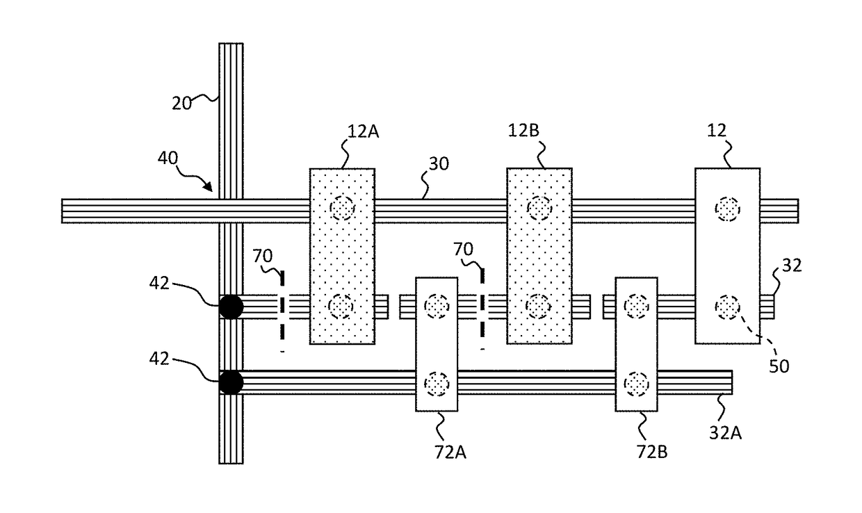
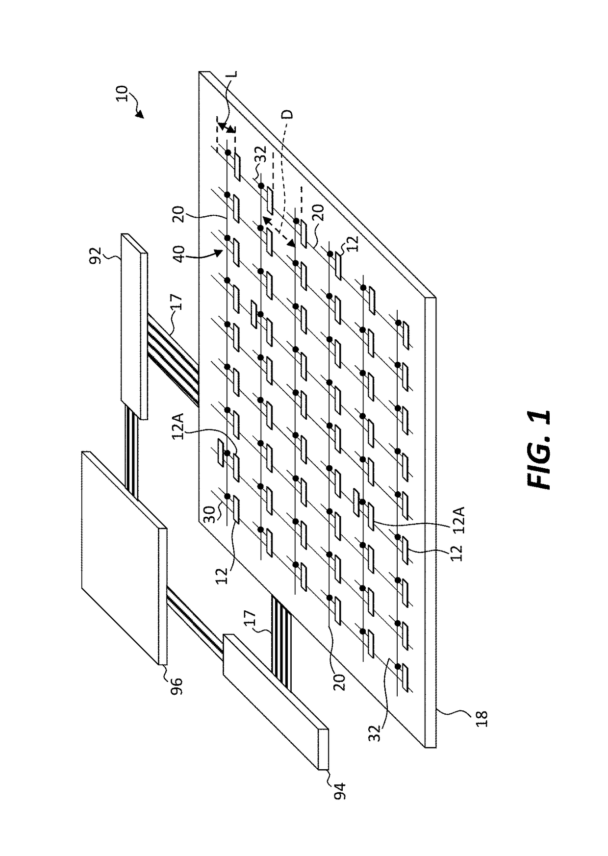
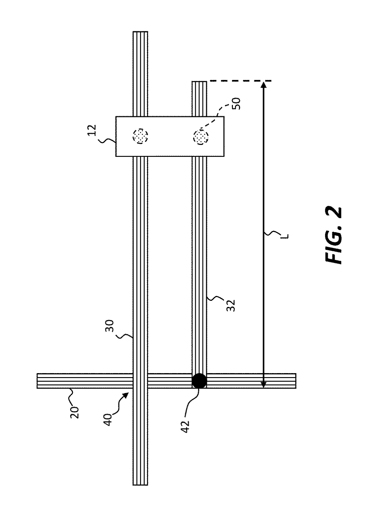
[0077]The present invention provides a robust structure and method for providing relatively small high-resolution matrix-addressed devices such as integrated circuit chiplets on a relatively large destination substrate and efficiently and cost-effectively electrically connecting them despite materials and manufacturing process variability and contamination. The structures and methods also provide a way to effectively repair matrix-addressed systems.

[0078]Referring to the perspective of FIG. 1, in an embodiment of the present invention, a repairable matrix-addressed system 10 includes a system substrate 18, an array of electrically conductive row lines 30 disposed over the system substrate 18, and an array of electrically conductive column lines 20 disposed over the system substrate 18. The system substrate 18 can be a multi-layer substrate with conductive wires in different layers. The row lines 30 extend over the system substrate 18 in a row direction and the column lines 20 extend...


PUM


Abstract

A repairable matrix-addressed system includes a system substrate, an array of electrically conductive row lines, and an array of electrically conductive column lines disposed over the system substrate. The row lines extend over the system substrate in a row direction and the column lines extend over the system substrate in a column direction different from the row direction to define an array of non-electrically conductive intersections between the row lines and the column lines. An array of electrically conductive line segments is disposed over the system substrate. The line segments extend over the system substrate substantially parallel to the row direction and have a line segment length that is less than the distance between adjacent column lines. Each line segment is electrically connected to a column line. One or more devices are electrically connected to each row line and to each line segment adjacent to the row line.

Description

RELATED APPLICATIONS[0001]This application claims priority to and the benefit of U.S. Provisional Patent Application No. 62 / 387,189, filed Dec. 23, 2015, titled Matrix-Addressed Device Repair, the contents of which are incorporated by reference herein in its entirety.[0002]Reference is made to commonly assigned U.S. patent application Ser. No. 14 / 743,788 entitled Micro Assembled LED Displays and Lighting Elements by Bower et al, U.S. patent application Ser. No. 14 / 822,864 entitled Chiplets with Connection Posts by Prevatte et al., and U.S. patent application Ser. No. 14 / 807,226 entitled Parallel Redundant Chiplet System by Cok et al., the disclosures of which are incorporated herein by reference in their entirety.FIELD OF THE INVENTION[0003]The present invention relates to structures and methods for providing robust and repairable matrix-addressed systems and to micro-transfer printing devices onto such matrix-addressed system.BACKGROUND OF THE INVENTION[0004]Substrates with electro...

Claims


Application Information

Patent Timeline
IPC IPC(8): H01L27/02H01L25/16H01L33/62H01L23/528H01L21/66
CPCH01L27/0207H01L23/528H01L22/32H01L2933/0066H01L33/62H01L25/167H01L22/14H01L28/00H10B43/27
Inventor COK, RONALD S.BOWER, CHRISTOPHERMEITL, MATTHEWTRINDADE, ANTONIO JOSE MARQUES
Owner X DISPLAY CO TECH LTD
Features
  • Generate Ideas
  • Intellectual Property
  • Life Sciences
  • Materials
  • Tech Scout
  • Unparalleled Data Quality
  • Higher Quality Content
  • 60% Fewer Hallucinations
Learn More