Transfer printed device repair

a printed device and transfer technology, applied in the field of transfer printed device repair, can solve the problems of waste of materials, low performance of other integrated circuits, and performance limitations of the technique, and achieve the effect of simple and robust electrical interconnections and high resolution

Active Publication Date: 2018-06-21
X DISPLAY CO TECH LTD
View PDF0 Cites 31 Cited by
  • Summary
  • Abstract
  • Description
  • Claims
  • Application Information

AI Technical Summary

Benefits of technology

[0023]In certain embodiments, the present invention enables, inter alia, large arrays of devices on a system substrate that are subject to manufacturing variability and provides simple and robust electrical interconnections. The devices can be transfer printed to a system substrate at a relative high resolution.

Problems solved by technology

This technique, although widely used in the display industry, has performance limitations.
Despite processing methods used to improve the performance of thin-film transistors, such transistors may provide performance that is lower than the performance of other integrated circuits formed in mono-crystalline semiconductor material.
Semiconductor material and active components can be provided only on portions of the substrate, leading to wasted material and increased material and processing costs.
The choice of substrate materials can also be limited by the processing steps necessary to process the semiconductor material and the photo-lithographic steps used to pattern the active components.
For example, plastic substrates have a limited chemical and heat tolerance and do not readily survive photo-lithographic processing.
Furthermore, the manufacturing equipment used to process large substrates with thin-film circuitry is relatively expensive.
However, such substrate materials can be more expensive, limited in size, or difficult to process.
While this approach can provide substrates with the same performance as integrated circuits, the size of such substrates may be limited, for example to a 12-inch diameter circle, the wafers are relatively expensive compared to other substrate materials such as glass, polymer, or quartz, and the wafers are rigid.
However, these techniques may be limited in the size of the integrated circuits that can be placed so that the integrated circuits and their packaging can be larger and more expensive than is desired.
In some cases, the source wafer or destination substrate can have particulate contamination that inhibits element transfer from the source wafer to the destination substrate by the stamp, for example due to process abnormalities or undesired particles on the stamp, the source wafer, or the destination substrate.
It is also possible that the elements themselves are defective due to materials or manufacturing process errors in the wafer.
Such problems can reduce manufacturing yields, increase product costs, and necessitate expensive repair or rework operations.
This process is expensive and requires a number of manufacturing steps.
Moreover, the topographical structure of the small integrated circuits over the destination substrate renders the electrical connections problematic, for example it can be difficult to form a continuous conductor from the destination substrate to the small integrated circuit because of the differences in height over the surface between the small integrated circuits and the destination substrate.
However, the smallest surface-mount device readily available is several hundred microns long and wide, precluding their use for applications requiring integrated circuits with circuit elements having a size of several microns, or less, for example.

Method used


Image

  • Transfer printed device repair
  • Transfer printed device repair
  • Transfer printed device repair

Examples


Embodiment Construction

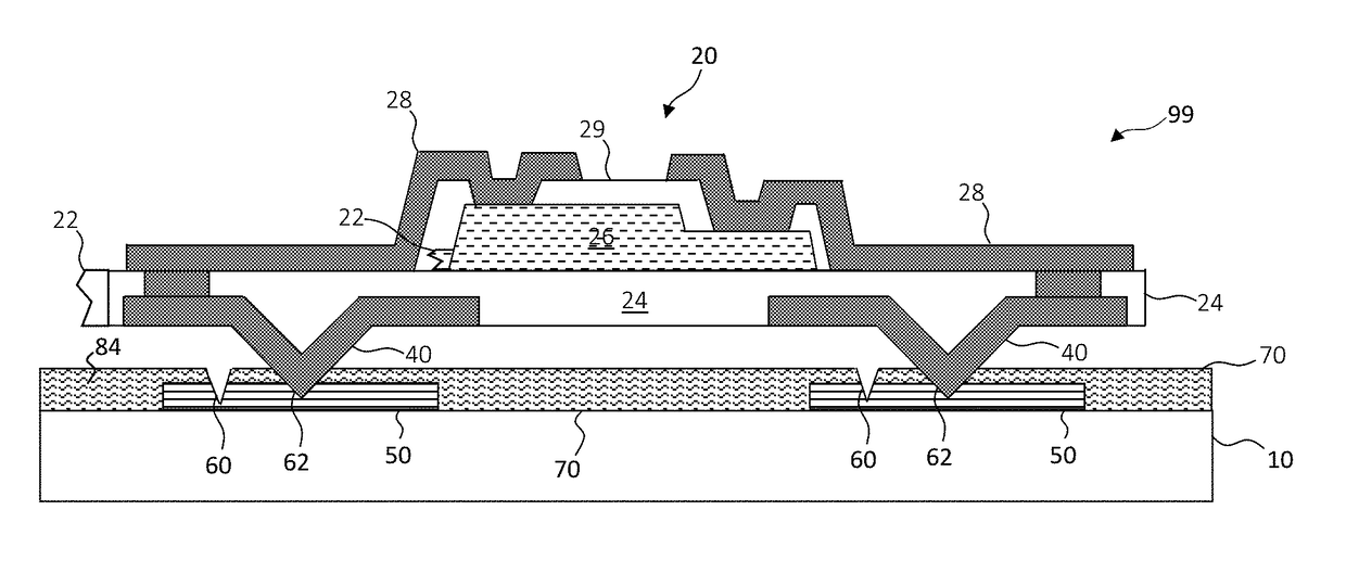
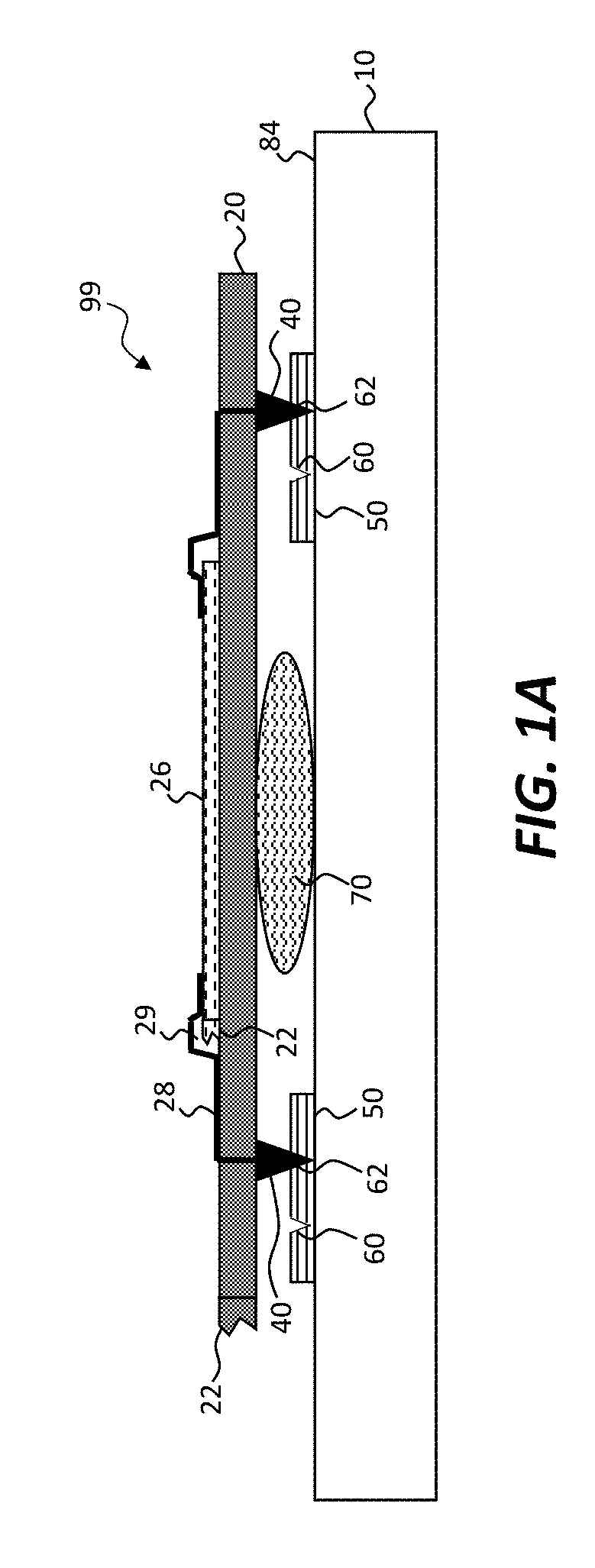
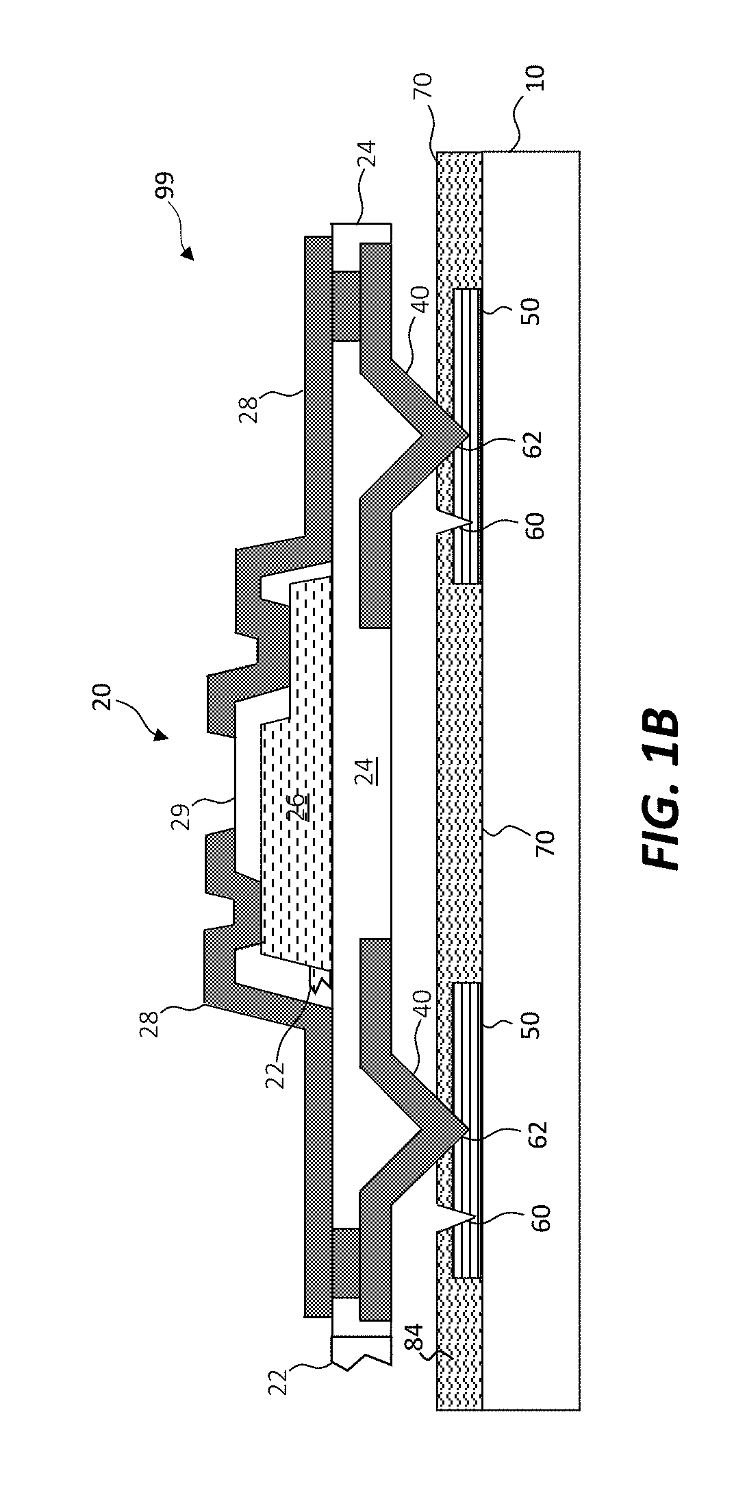
[0055]The present invention provides, inter alia, structures and methods that enable large, high-yield, cost-effective, and electrically connected arrays of relatively small integrated circuit chiplets or assemblies at a high resolution on a relatively large destination substrate despite materials and manufacturing process variability and contamination.

[0056]Referring to FIGS. 1A and 1B, in some embodiments of the present invention, a repaired transfer-printed system 99 includes a system substrate 10. Two or more contact pads 50 are disposed on the system substrate 10 and one or more micro-transfer printed devices 20 are disposed in contact with the contact pads 50 or system substrate 10. Each device 20 has two or more connection posts 40. Each connection post 40 is in physical and electrical contact with a contact pad 50 and forms a second imprint 62 in the physically contacted contact pad 50, for example by piercing or deforming the physically contacted contact pad 50.

[0057]At lea...


PUM


Abstract

A repaired transfer printed system (e.g., micro-transfer printed system) includes a system substrate having two or more contact pads disposed on the system substrate. One or more transfer printed devices (e.g., micro-transfer printed devices) are disposed in contact with the system substrate, each device having two or more connection posts. Each connection post of a replacement device is in physical contact with a contact pad, the connection post forming a second imprint in the physically contacted contact pad. In certain embodiments, a first imprint is in at least one of the physically contacted contact pads and is between the replacement device and the system substrate.

Description

PRIORITY APPLICATION[0001]This application claims the benefit of U.S. Provisional Patent Application No. 62 / 436,240, filed Dec. 19, 2016, entitled Micro-Transfer Printed Device Repair, the content of which is hereby incorporated by reference herein in its entirety.CROSS REFERENCE TO RELATED APPLICATIONS[0002]Reference is made to commonly assigned U.S. patent application Ser. No. 14 / 743,788 to Bower et al., entitled Micro Assembled LED Displays and Lighting Elements and filed Jun. 18, 2015, U.S. patent application Ser. No. 14 / 822,864 to Prevatte et al., entitled Chiplets with Connection Posts and filed Aug. 10, 2015, U.S. patent application Ser. No. 14 / 807,226 to Cok et al., entitled Parallel Redundant Chiplet System and filed Jul. 23, 2015, U.S. Provisional Patent Application No. 62 / 317,107 to Bower et al., entitled Pressure Activated Electrical Interconnection by Micro-Transfer Printing and filed Apr. 1, 2016, and U.S. patent application Ser. No. 15 / 040,810 to Cok et al., entitled ...

Claims


Application Information

Patent Timeline
Patent Type & Authority Applications(United States)
IPC IPC(8): H01L21/66H01L23/00
CPCH01L22/22H01L24/799H01L24/98H01L2224/98H01L2224/7999H01L2224/13186H01L24/13H01L24/16H01L24/81H01L2224/13562H01L2224/1357H01L2224/136H01L2224/16238H01L2224/95001H01L2224/95136H01L25/0753H01L33/62H01L2924/053H01L2924/00014
Inventor COK, RONALD S.RADAUSCHER, ERICHGOMEZ, DAVID
Owner X DISPLAY CO TECH LTD
Why Eureka
Try Eureka