Supercharge Your Innovation With Domain-Expert AI Agents!

Method for Reduced Load Memory Module

a memory module and load reduction technology, applied in memory systems, memory adressing/allocation/relocation, instruments, etc., can solve problems such as reducing the operational speed of communication with such dimming, affecting the performance of memory modules, so as to reduce load and reduce load. load, reduce load for coupling, the effect of sufficient load reduction

Active Publication Date: 2017-07-27
INVENSAS CORP
View PDF2 Cites 2 Cited by
  • Summary
  • Abstract
  • Description
  • Claims
  • Application Information

AI Technical Summary

Benefits of technology

This design enables multiple memory modules to share a memory channel with minimal performance impact, reducing latency and complexity compared to buffered solutions, while maintaining high data transfer rates.

Problems solved by technology

For example, if one DIMM is coupled via one channel, the loading effects may not be appreciably large to prevent higher-stock or over-clocking speeds for operation.
However, if a second DIMM is added to that same memory channel in this example, then loading effects caused by addition of such second DIMM can substantially reduce operational speed for communication with such DIMMs.
This problem may become worse with each additional memory module added onto a channel.
However, adding support for additional channels complicates both processor design and motherboard design.
However, buffering not only adds additional circuitry, which may be in the form of additional chips, to a memory module, such buffering may also increase operational latency of a memory module in comparison to an unbuffered memory module, such as a UDIMM for example.
Thus, if only one memory module is located on a channel, a load reduced memory module may be slower than a more conventional unbuffered memory module.

Method used


Image

  • Method for Reduced Load Memory Module
  • Method for Reduced Load Memory Module
  • Method for Reduced Load Memory Module

Examples


Embodiment Construction

[0024]In the following description, numerous specific details are set forth to provide a more thorough description of the specific examples described herein. It should be apparent, however, to one skilled in the art, that one or more other examples or variations of these examples may be practiced without all the specific details given below. In other instances, well known features have not been described in detail so as not to obscure the description of the examples herein. For ease of illustration, the same number labels are used in different diagrams to refer to the same items; however, in alternative examples the items may be different.

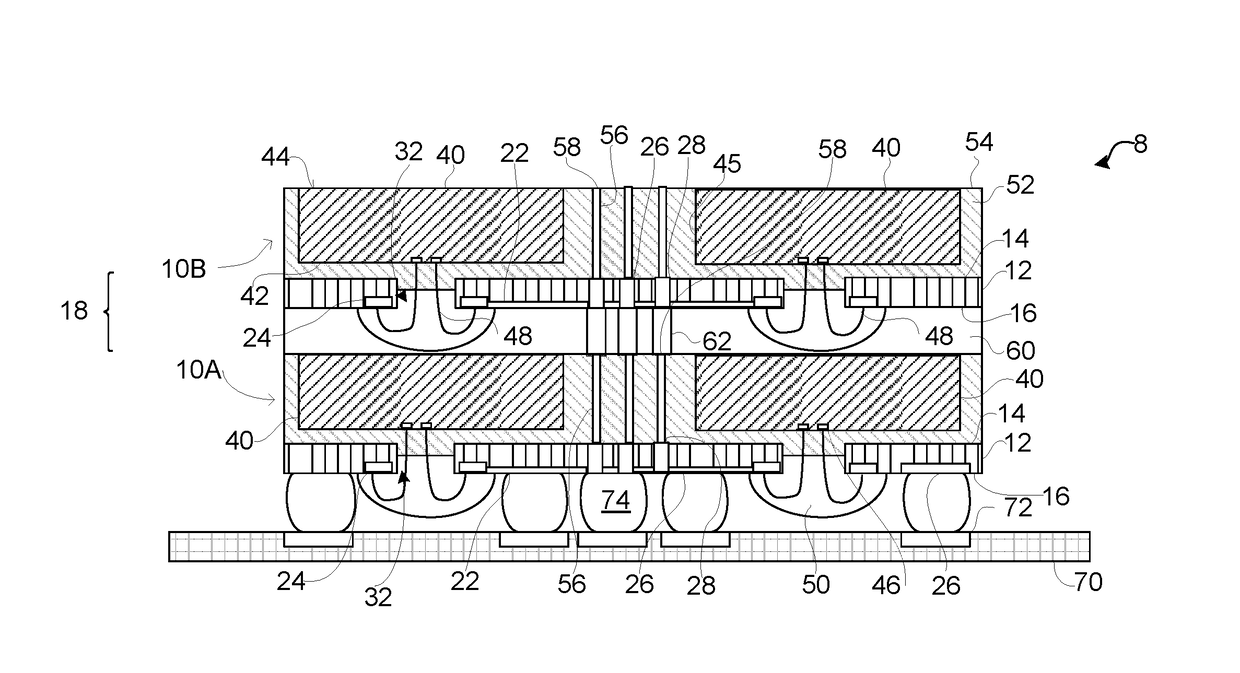
[0025]FIG. 1 is a cross-sectional view of an assembly 8. Assembly 8 may include microelectronic packages 10A and 10B. Assembly 8 may be a memory chip 8, and microelectronic packages 10A and 10B may be separated to provide memory chips 8 or may be packaged together as a single memory chip 8. Microelectronic packages 10A and 10B may be coupled to cir...


PUM


Abstract

A method for reducing load in a memory module. In such a method, a plurality of memory chips are coupled to a circuit platform. Each memory chip of the plurality of memory chips each has a plurality of memory dies. At least one controller is coupled to the circuit platform and further coupled to the plurality of memory chips for communication with the plurality of memory dies thereof. The at least one controller is for receiving chip select signals to provide a plurality of rank select signals in excess of the chip select signals. The plurality of memory dies are coupled with wire bonds within the plurality of memory chips for a reduced load for coupling the circuit platform for communicating via a memory channel. The load is sufficiently reduced for having at least two instances of the memory module share the memory channel.

Description

FIELD CROSS-REFERENCE TO RELATED APPLICATION(S)[0001]This application is a divisional of, and hereby claims priority to, pending U.S. patent application Ser. No. 14 / 645,811, filed on Mar. 12, 2015, the entirety of which is hereby incorporated by reference herein for all purposes.FIELD[0002]The following description relates to memory modules. More particularly, the following description relates to a reduced load memory module.BACKGROUND[0003]In the computer industry, on-board memory is conventionally coupled to a processor through a memory channel. Along those lines, a motherboard may have multiple memory slots for multiple memory modules, such as SIMMs or DIMMs, for a channel. More recently, processors are capable of handling more than one memory channel. Some processors are capable of being coupled to two or four memory channels.[0004]One reason for going to multiple channels is to effectively reduce loading effects for operation at higher memory interface speeds. For example, if o...

Claims


Application Information

Patent Timeline
Patent Type & Authority Applications(United States)
IPC IPC(8): G06F13/16G06F12/06
CPCG06F13/1673G06F13/1694G06F12/0623G11C5/04H01L2224/4824H01L2924/15311G11C8/06G11C5/06G11C8/12G06F12/00
Inventor SUN, ZHUOWENCHEN, YONG
Owner INVENSAS CORP
Features
  • R&D
  • Intellectual Property
  • Life Sciences
  • Materials
  • Tech Scout
  • Unparalleled Data Quality
  • Higher Quality Content
  • 60% Fewer Hallucinations
Learn More