Bonding film

a bonding film and film technology, applied in the field of bonding films, can solve problems such as weak signal reception

Active Publication Date: 2017-08-10
HU DYI CHUNG
View PDF3 Cites 18 Cited by
  • Summary
  • Abstract
  • Description
  • Claims
  • Application Information

AI Technical Summary

Problems solved by technology

The disadvantage for the prior art is that the longer

Method used


Image

  • Bonding film
  • Bonding film
  • Bonding film

Examples


first embodiment

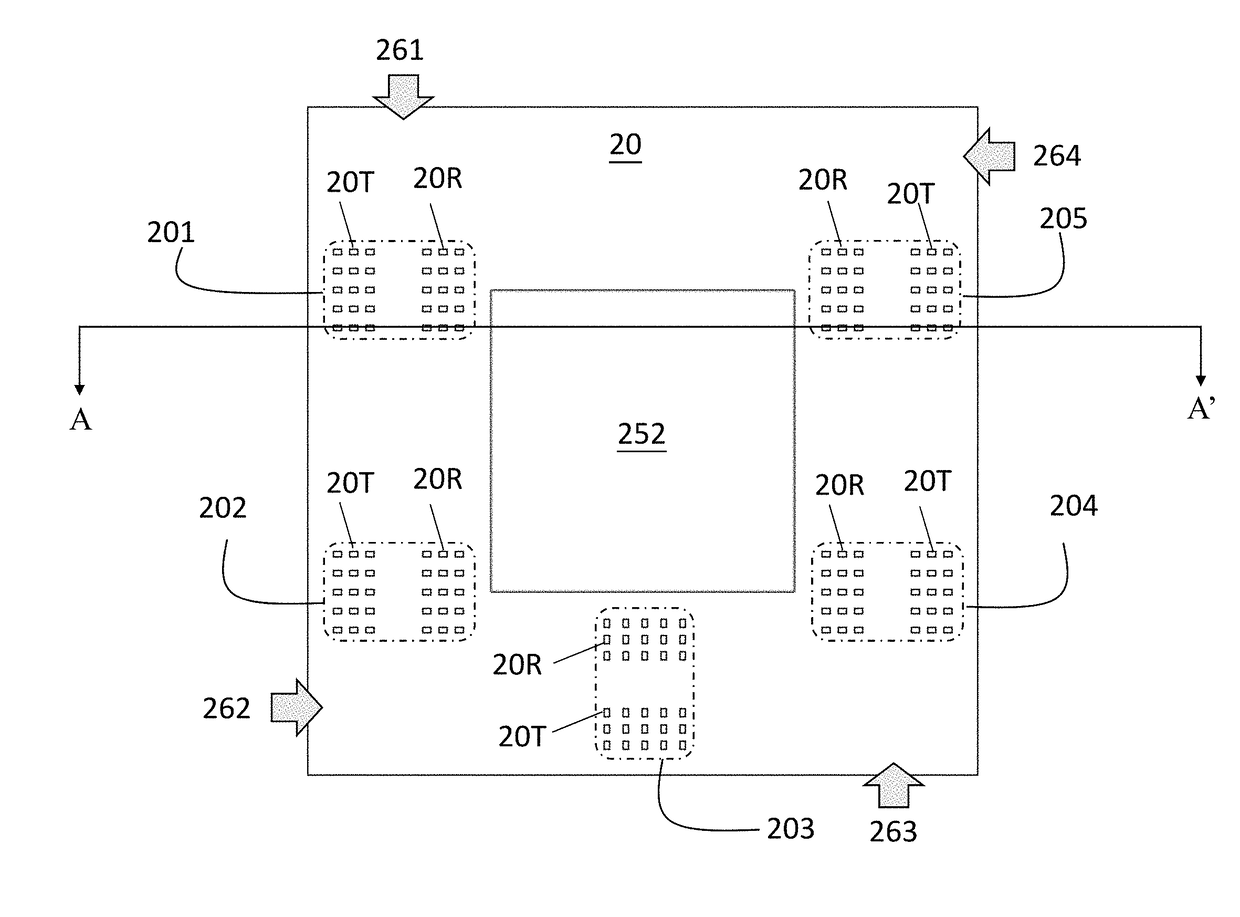
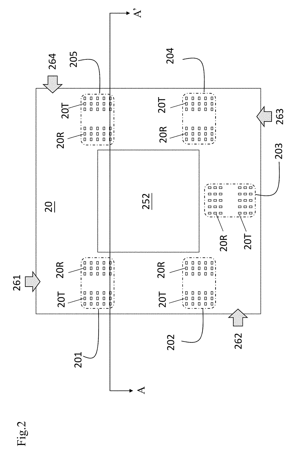
[0024]FIG. 2 shows a first embodiment according to the present invention.

[0025]FIG. 2 shows that a bonding film 20 comprises a left longitudinal branch 261, a lower latitudinal branch 262, a right longitudinal branch 263, and an upper latitudinal branch 264. The left longitudinal branch 261 has a lower end connected with a left end of the lower latitudinal branch 262. The right longitudinal branch 263 has a lower end connected with a right end of the lower latitudinal branch 262. The upper latitudinal branch 264 has a left end connected with an upper end of the left longitudinal branch 261, and has a right end connected with an upper end of the right longitudinal branch 263.

[0026]A first bonding area 201 and a second bonding area 202 are configured in the left longitudinal branch 261. A third bonding area 203 is configured in the lower latitudinal branch 262. A fourth bonding area 204 and a fifth bonding area 205 are configured in the right longitudinal branch 263. A plurality of ou...

third embodiment

[0045]FIG. 9 shows a third embodiment according to the present invention.

[0046]FIG. 9 shows that an L shaped bonding film 40 is formed with a left longitudinal branch 261, and a lower latitudinal branch 262. The L shaped bonding film 40 has a plurality of outer bonding pads 20T and a plurality of inner bonding pads 20R exposed on top side of the L shaped bonding film 40. The two branches 261, 262, forms an L shaped bonding film 40. The L shaped bonding film 40 provides left side, and lower side accommodation for chips 401, 402, each on one side of the two sides, so that a central chip 400 is able to electrically couple to the peripheral chips 401, 402 through the inner bonding pads 20R and the outer bonding pads 20T of the L shaped bonding film 40.

fourth embodiment

[0047]FIG. 10 shows a fourth embodiment according to the present invention.

[0048]FIG. 10 shows that the bonding film 20 further comprises bottom contact 23A which is able to electrically couple to a top metal contact 23B of the redistribution circuitry of the redistribution layer RDL12 on bottom when the bonding film 20 is embedded in the redistribution substrate.

[0049]FIGS. 11A˜11C show a top view for the three embodiments according to the present invention.

[0050]FIG. 11A shows that the central portion 282 of the redistribution layer RDL12 is configured in the central opening of the bonding film 20. The top redistribution layer RDL11 wraps around an outer periphery of the bonding film 20.

[0051]FIG. 11B shows that the central portion 282 of the redistribution layer RDL12 is configured in the central opening of the U shaped bonding film 30. The top redistribution layer RDL11 wraps around an outer periphery of the U shaped bonding film 30.

[0052]FIG. 11C shows that the central portion ...


PUM


Abstract

A bonding film has at least a left longitudinal branch, and a lower latitudinal branch; a first bonding area is configured in a first branch, and a second bonding area is configured in a second branch. A plurality of outer top metal pads and a plurality of inner top metal pads are exposed on a top surface within each bonding area. A central chip is configured in a central area of the bonding film and is electrically coupled to the inner top metal pad, and at least two peripheral chips are configured neighboring to the central chip and electrically coupled to the outer top metal pads. Each of the inner top metal pads is electrically coupled to a corresponding outer top metal pad through an embedded circuitry. The central chip communicates with the peripheral chips through the inner top metal pad, embedded circuitry, and outer top metal pad of the bonding film.

Description

BACKGROUND[0001]Technical Field[0002]The present invention relates to a bonding film, especially relates to a bonding film for signal communication between a central chip and peripheral chips through a circuitry of the bonding film.[0003]Description of Related Art[0004]FIG. 1 shows a prior art.[0005]FIG. 1 shows that a first chip 11 and a second chip 12 are configured on a top side of an interposer 111. The interposer 111 is configured on a top side of a package substrate 112. The package substrate 112 is configured on a system board 113. For signal communication between the first chip 11 and the second chip 12, a long path needs to go as indicated by the dash line 15. Referring to FIG. 1, the communication path from chip 11 to chip 12 goes from the circuitry of the interposer 111, package substrate 112, system board 113, back to the package substrate 112, the interposer 111, and then reaches chip 12.[0006]The disadvantage for the prior art is that the longer the path it goes, the w...

Claims


Application Information

Patent Timeline
IPC IPC(8): H01L23/00H01L25/065
CPCH01L24/08H01L25/0657H01L25/0655H01L2224/023H01L24/25H01L24/03H01L24/35H01L24/37H01L2224/35H01L2224/3701H01L2224/0401H01L2224/73204H01L2924/15192H01L2924/15311H01L2924/18161H01L23/49816H01L23/49827H01L23/5384H01L23/5385H01L23/5386H01L2224/16225H01L2224/32225H01L2224/1403H01L2924/00H01L23/49822
Inventor HU, DYI-CHUNG
Owner HU DYI CHUNG
Why Eureka
Try Eureka