Process method and structure for high voltage mosfets

a technology of mosfets and process methods, which is applied in the direction of semiconductors, electrical devices, transistors, etc., can solve the problems of increasing manufacturing costs, increasing manufacturing costs, and reducing the control of the formation of dopant regions, so as to achieve the effect of reducing manufacturing costs and high energy

Active Publication Date: 2017-08-17
ALPHA & OMEGA SEMICON INC
View PDF7 Cites 0 Cited by
  • Summary
  • Abstract
  • Description
  • Claims
  • Application Information

AI Technical Summary

Benefits of technology

[0009]It is therefore an aspect of the present invention to provide a new and improved method of manufacturing for implanting the trench sidewall P-type dopant regions without requiring an additional implanting mask and without requiring a high energy dopant implant such that the cost of manufacturing can be reduced, whereby the above discussed limitations and difficulties can be resolved.
[0010]Specifically, it is an aspect of this invention that the implanting process takes advantage of the special configuration of the sidewalls at the trench endpoints where the sidewall perpendicular to the longitudinal direction of the trench is inherently exposed to open space as part of the trenches. Therefore, a P-type dopant region implanted through this endpoint sidewall can be carried out to reach the bottom P-type dopant region formed at the bottom of the trench without requiring the application of high energy dopant ions because the dopant ions are projected only through open space of the trenches without requiring penetrating through the semiconductor substrate. The PCOM dopant regions linking the P-type body regions formed at the top surface of the semiconductor substrate and the trench bottom P-type dopant regions are therefore formed only at the sidewalls of the trench endpoint. In contrast to the conventional methods, cost savings are achieved without requiring a high energy dopant implant.
[0012]It is another aspect of this invention that the sidewall dopant implant through the open space along the longitudinal direction of the trench onto a trench sidewall at the trench endpoint, trench bend and trench notch provides better control over the implanting process. The device performance parameters are more accurately controllable and manufacturing variations caused by uncertainties due to high energy dopant implant to penetrate through substrate are reduced.

Problems solved by technology

Conventional methods of manufacturing high voltage (HV) MOSFET devices are encountered with difficulties and limitations to further improve the performances due to different tradeoffs.
The requirements of additional mask and the processes of applying high energy dopant ions cause the increase of the manufacturing costs.
Additionally, high energy implantations into the bottom portions of the trench sidewalls followed with a diffusion process generally have less control of the formation of the dopant regions.
These uncertainties of the manufacturing processes result in greater variations of device performance and less accurate control of the manufacturing qualities.
The manufacturing costs are increased due to the additional mask and high energy implant requirements.

Method used


Image

  • Process method and structure for high voltage mosfets
  • Process method and structure for high voltage mosfets
  • Process method and structure for high voltage mosfets

Examples


Embodiment Construction

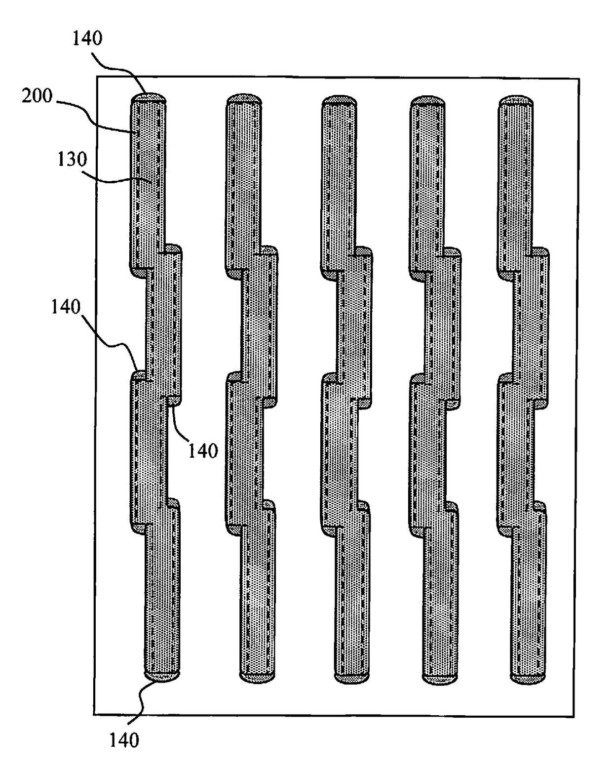
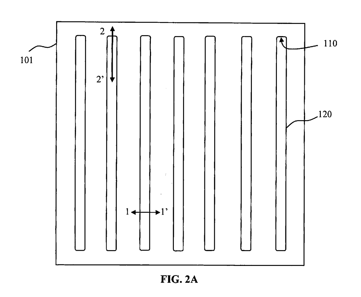
[0029]FIG. 2A is a top view of a conventional trench configuration on a semiconductor substrate. FIGS. 2B, 2C-1, 2C-2, 2D-1, 2D-2, 2E-1, 2E-2, 2F-1, 2F-2, 2G-1, 2G-2, 2H-1 and 2H-2 are side cross sectional views illustrating the processing steps of forming the PCOM structural configuration along the line 1-1′ and line 2-2′ in FIG. 2A respectively in different embodiments of the present invention.

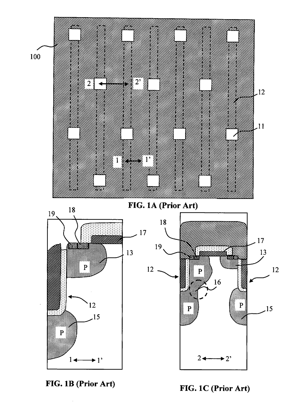
[0030]As shown in FIG. 2A, a plurality of trenches 120 are formed on a semiconductor substrate 101 with each trench 120 having a trench endpoint sidewall 110. The plurality of trenches 120 can be formed as follow: an oxide hard mask 111 is deposited atop the semiconductor substrate as shown in FIG. 2B; then the hard mask 111 is patterned according to a pre-determined configuration similar as the that shown in FIG. 2A; and the semiconductor substrate 101 is then anisotropically etched out through the patterned hard mask 111 to form the a plurality of trenches 120 with each trench 120 having t...


PUM


Abstract

This invention discloses a semiconductor power device disposed in a semiconductor substrate. The semiconductor power device comprises a plurality of trenches formed at a top portion of the semiconductor substrate extending laterally across the semiconductor substrate along a longitudinal direction each having a nonlinear portion comprising a sidewall perpendicular to a longitudinal direction of the trench and extends vertically downward from a top surface to a trench bottom surface. The semiconductor power device further includes a trench bottom dopant region disposed below the trench bottom surface and a sidewall dopant region disposed along the perpendicular sidewall wherein the sidewall dopant region extends vertically downward along the perpendicular sidewall of the trench to reach the trench bottom dopant region and pick-up the trench bottom dopant region to the top surface of the semiconductor substrate.

Description

CROSS REFERENCE TO OTHER APPLICATIONS[0001]This application is a Continuation-In-Part (CIP) of and claims priority to U.S. patent application Ser. No. 13 / 892,191 entitled “A PROCESS METHOD AND STRUCTURE FOR HIGHVOLTAGE MOSFETS,” filed May 10, 2013, which is incorporated herein by reference for all purposes.BACKGROUND OF THE INVENTION[0002]1. Field of the Invention[0003]The invention relates generally to the manufacturing processes and structures of semiconductor power devices. More particularly, this invention relates to simplified manufacturing processes and structural configurations of improved high voltage (HV) metal oxide semiconductor field effect transistors (MOSFET).[0004]2. Description of the Prior Art[0005]Conventional methods of manufacturing high voltage (HV) MOSFET devices are encountered with difficulties and limitations to further improve the performances due to different tradeoffs. In the vertical semiconductor power devices, there is a tradeoff between the drain to s...

Claims


Application Information

Patent Timeline
Patent Type & Authority Applications(United States)
IPC IPC(8): H01L29/06H01L29/78H01L21/265H01L29/739
CPCH01L29/0696H01L21/26586H01L29/7813H01L29/7397H01L29/0623H01L29/407H01L29/66333H01L29/1095H01L29/66712H01L29/7802H01L29/7395H01L29/66348H01L29/66666
Inventor DING, YANGPINGLUI, SIKBOBDE, MADHURZHANG, LEIKIM, JONGOHCHEN, JOHN
Owner ALPHA & OMEGA SEMICON INC
Why Eureka
Try Eureka