

Method of manufacture for single crystal acoustic resonator devices using micro-vias
a manufacturing method and technology of acoustic wave resonators, applied in the field of electronic devices, can solve the problems of rf complexity in driving smartphones and limitations of conventional rf technology, and achieve the effect of simple and cost-effectiv
- Summary
- Abstract
- Description
- Claims
- Application Information
AI Technical Summary
Benefits of technology
Problems solved by technology
Method used
Image

Examples
Embodiment Construction
[0038]According to the present invention, techniques generally related to electronic devices are provided. More particularly, the present invention provides techniques related to a single crystal acoustic resonator using wafer level technologies. Merely by way of example, the invention has been applied to a resonator device for a communication device, mobile device, computing device, among others.
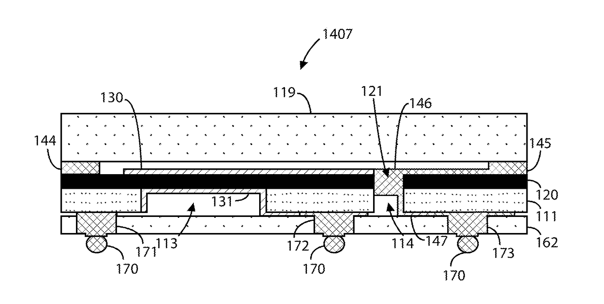
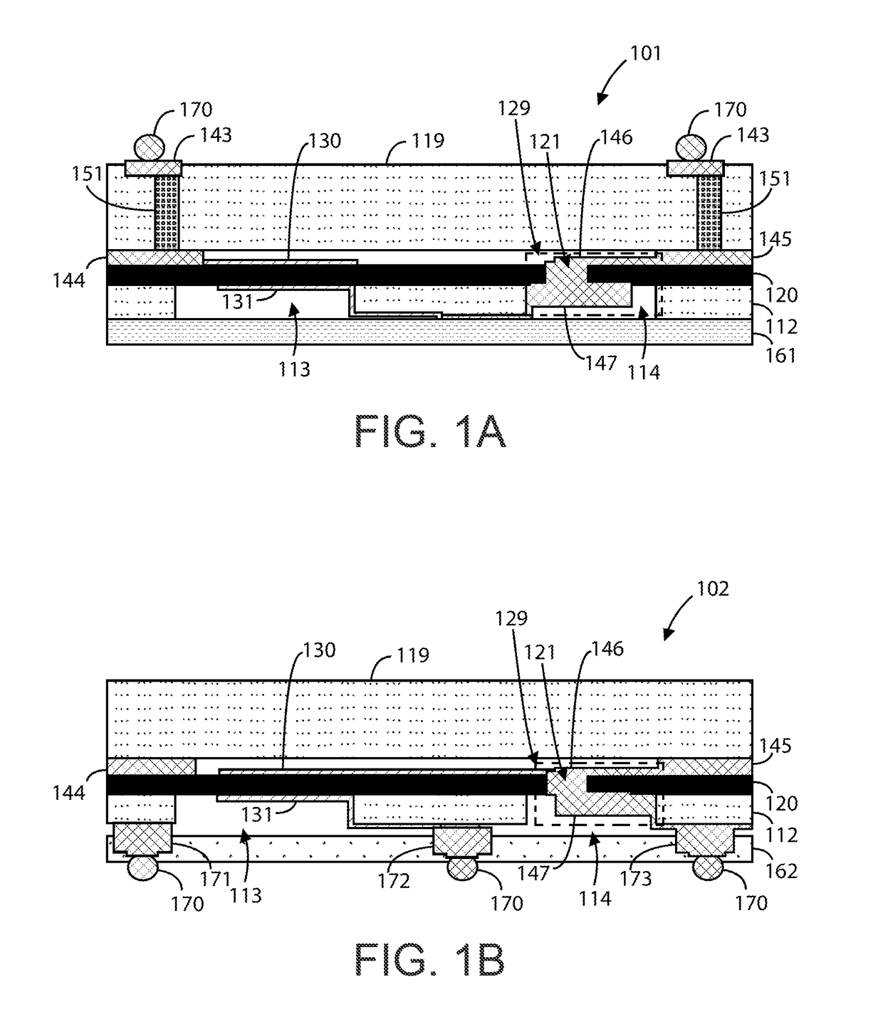
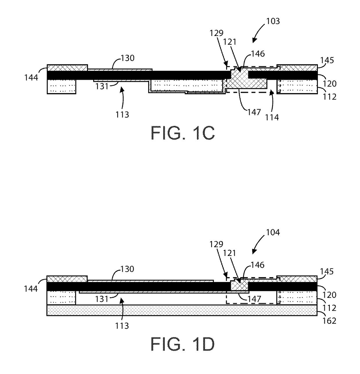
[0039]FIG. 1A is a simplified diagram illustrating an acoustic resonator device 101 having topside interconnections according to an example of the present invention. As shown, device 101 includes a thinned seed substrate 112 with an overlying single crystal piezoelectric layer 120, which has a micro-via 129. The micro-via 129 can include a topside micro-trench 121, a topside metal plug 146, a backside trench 114, and a backside metal plug 147. Although device 101 is depicted with a single micro-via 129, device 101 may have multiple micro-vias. A topside metal electrode 130 is formed overlyi...
PUM
| Property | Measurement | Unit |
|---|---|---|
| Temperature | aaaaa | aaaaa |
| Temperature | aaaaa | aaaaa |
| Thickness | aaaaa | aaaaa |
Abstract
Description
Claims
Application Information