
Eureka
For R&D, Eureka makes reading and utilizing patents & technical documents easy.
Eureka AIR
Designed for self-driven R&D workflows. Generate viable solutions, solve complex R&D challenges, empower your innovation with AI.

Eureka Materials
Designed for material experts only. Revolutionize your material R&D, from search, analyze, to developing new materials.

TechResearch
Generate reliable direction feasibility study reports for your R&D in just a few steps.

TechSeek
Discover and master advanced knowledge NOW. Basics, ideas, possibilities, all at once.

TechMind
As an expert in R&D Theories, TechMind can generates customized viable solutions instantly.

TechRisk
Analyze your overall solution with one click, know your potential R&D risks in advance.

TechMonitor
Get weekly tech updates, stay abreast of the latest tech innovations and key insights.
Development method, development device, and non-transitory computer-readable storage medium
- Summary
- Abstract
- Description
- Claims
- Application Information
AI Technical Summary
Benefits of technology
Problems solved by technology
Method used
Image

Examples
Example
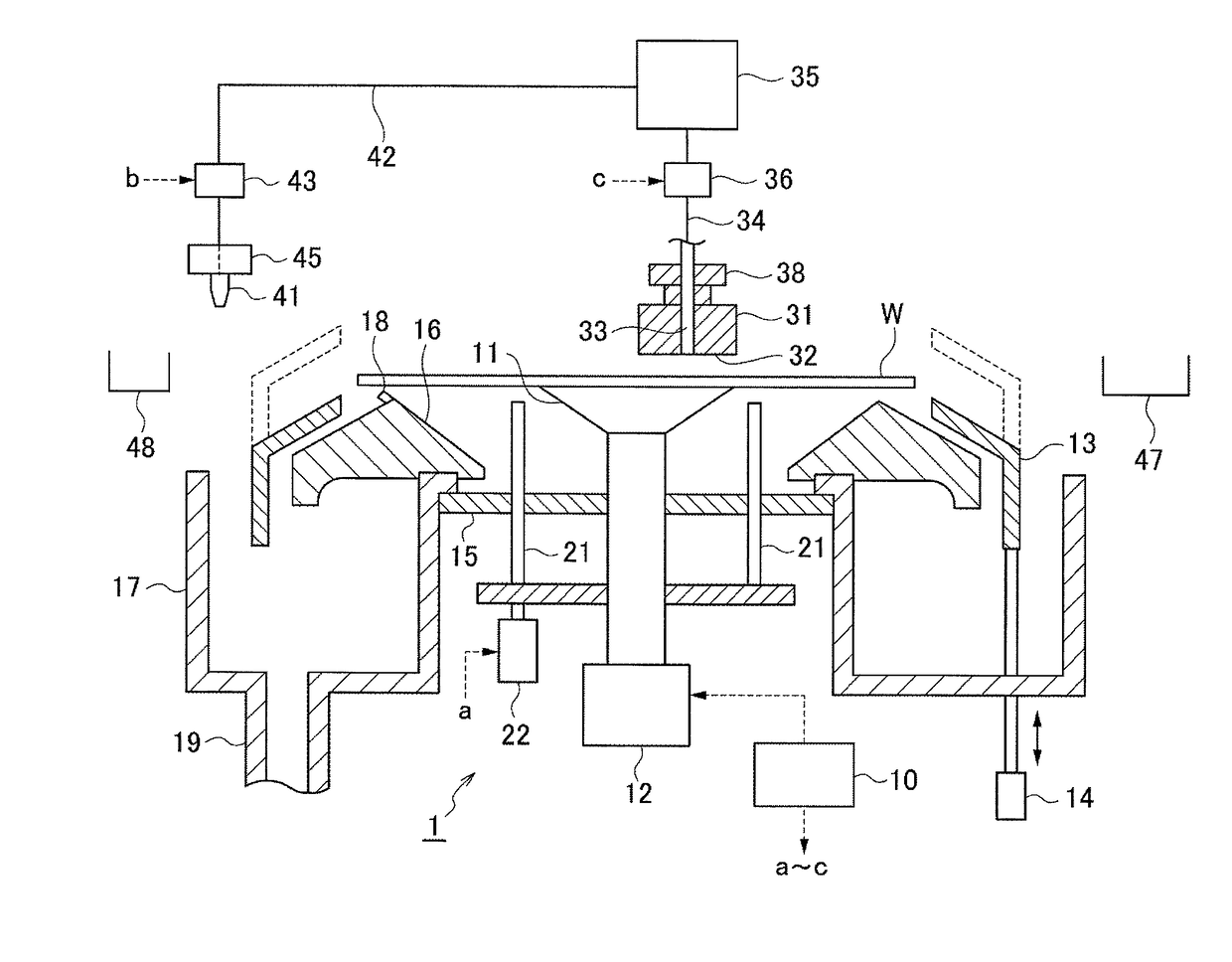
[0027]A development device 1 according to an embodiment of the present invention will be described below referring to a vertical sectional side view of FIG. 1 and a horizontal sectional plan view of FIG. 2. The development device 1 performs a development process on a wafer W which is a substrate for manufacturing a semiconductor device that has undergone formation of a resist film of a negative photoresist on its front surface and exposure of the resist film. The reference character 11 in the drawings represents a spin chuck serving as a substrate holding unit. The spin chuck 11 vacuum-sucks a central part of a back surface of the wafer W to horizontally holds a wafer W. The reference character 12 represents a rotating mechanism for rotating the spin chuck 11 and thereby rotating the wafer W held by the spin chuck 11 around the central axis of the wafer W. The rotating mechanism 12 is capable of switching the direction of rotation. Clockwise rotation and counterclockwise rotation of...
PUM
 Abstract
Description
Claims
Application Information
 - R&D Engineer
- R&D Manager
- IP Professional
- Industry Leading Data Capabilities
- Powerful AI technology
- Patent DNA Extraction
Browse by: Latest US Patents, China's latest patents, Technical Efficacy Thesaurus, Application Domain, Technology Topic, Popular Technical Reports.
© 2024 PatSnap. All rights reserved.Legal|Privacy policy|Modern Slavery Act Transparency Statement|Sitemap|About US| Contact US: help@patsnap.com