Semiconductor devices

a technology of semiconductors and devices, applied in the direction of semiconductor devices, basic electric elements, electrical equipment, etc., can solve problems such as leakage current vulnerability, and achieve the effects of reducing parasitic capacitance between gate structures, good electrical characteristics, and reducing leakage current through gate spacer structures

Inactive Publication Date: 2017-11-02
SAMSUNG ELECTRONICS CO LTD
View PDF0 Cites 30 Cited by
  • Summary
  • Abstract
  • Description
  • Claims
  • Application Information

AI Technical Summary

Benefits of technology

[0008]In the semiconductor device in accordance with example embodiments, the gate spacer structure may include the offset pattern having a dielectric constant lower than that of silicon nitride or silicon oxycarbonitride, and having a band gap higher than that of silicon nitride or silicon oxycarbonitride. Thus, a leakage current through the gate spacer structure may be reduced, and a parasitic capacitance between the gate structures may be reduced. Accordingly, the semiconductor device may have good electrical characteristics.

Problems solved by technology

Silicon nitride may have a high dielectric constant and low band gap energy, and thus may be vulnerable to leakage current.

Method used


Image

  • Semiconductor devices
  • Semiconductor devices
  • Semiconductor devices

Examples


Embodiment Construction

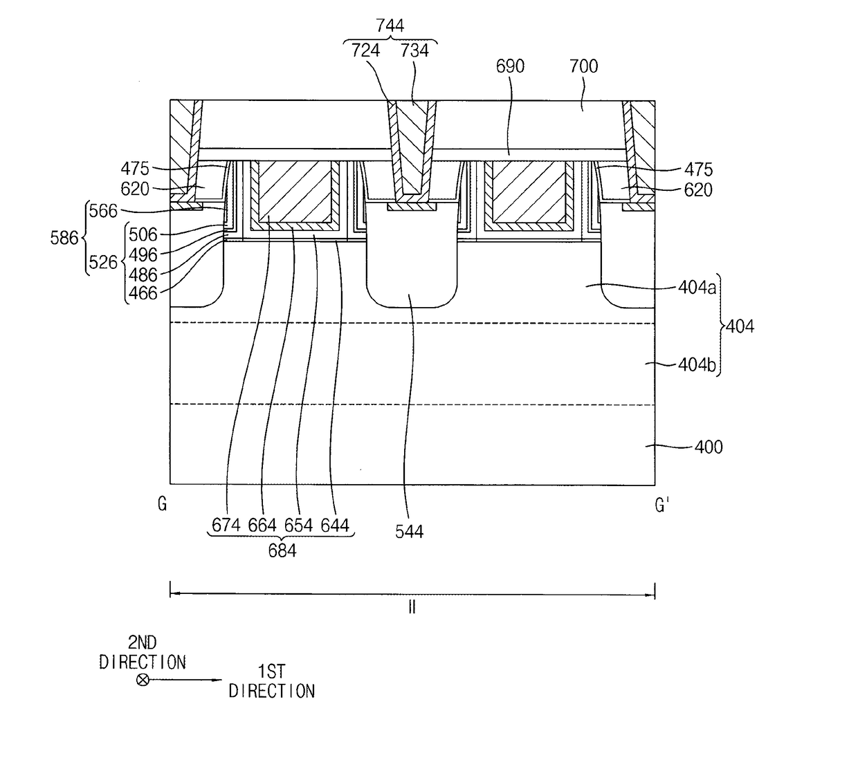
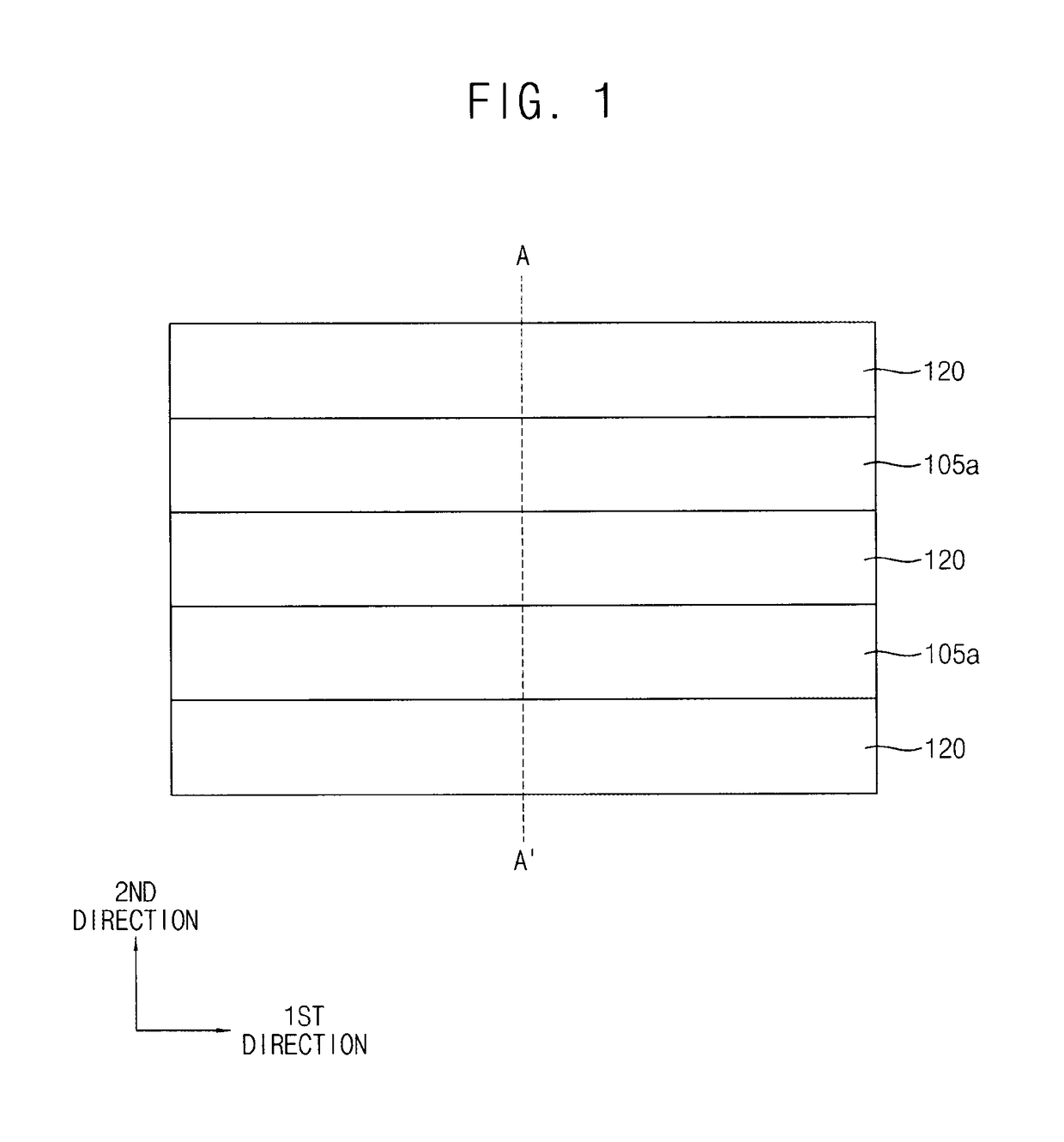
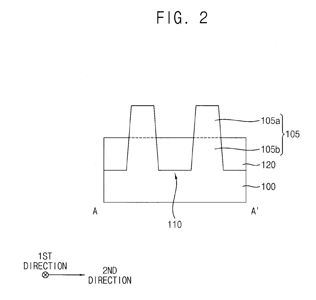
[0014]FIGS. 1 to 36 are plan views and cross-sectional views illustrating stages of a method of manufacturing a semiconductor device in accordance with example embodiments. Particularly, FIGS. 1, 3, 6, 9, 13, 17, 22, 25, 27, 30 and 33 are plan views, and FIGS. 2, 4-5, 7-8, 10-12, 14-16, 18-21, 23-24, 26, 28-29, 31-32 and 34-36 are cross-sectional views.

[0015]FIGS. 2, 7, 10, 14, 16, 18, 20, 23, 31 and 34 are cross-sectional views taken along lines A-A′ of corresponding plan views, respectively, FIGS. 4, 28 and 35 are cross-sectional views taken along lines B-B′ of corresponding plan views, respectively, and FIGS. 5, 8, 11, 12, 15, 19, 21, 24, 26, 29, 32 and 36 are cross-sectional views taken along lines C-C′ of corresponding plan views, respectively.

[0016]Referring to FIGS. 1 and 2, an upper portion of a substrate 100 may be partially etched to form a first recess 110, and an isolation pattern 120 may be formed to fill a lower portion of the first recess 110.

[0017]The substrate 100 m...


PUM


Abstract

A semiconductor device includes an active fin on a substrate, a gate structure on the active fin, a gate spacer structure directly on a sidewall of the gate structure, and a source / drain layer on a portion of the active fin adjacent the gate spacer structure. The gate spacer structure includes a silicon oxycarbonitride (SiOCN) pattern and a silicon dioxide (SiO2) pattern sequentially stacked.

Description

CROSS-REFERENCE TO RELATED APPLICATION[0001]This application claims priority under 35 USC §119 to Korean Patent Application No. 10-2016-0051912, filed on Apr. 28, 2016 in the Korean Intellectual Property Office (KIPO), the contents of which are herein incorporated by reference in their entirety.BACKGROUND1. Field[0002]Example embodiments relate to semiconductor devices. For example, at least some example embodiments relate to semiconductor devices including spacers on sidewalls of a gate structure.2. Description of the Related Art[0003]A finFET may have a spacer on a sidewall of a gate structure, and the spacer may include a nitride, e.g., silicon nitride. Silicon nitride may have a high dielectric constant and low band gap energy, and thus may be vulnerable to leakage current.SUMMARY[0004]Example embodiments provide a semiconductor device having good characteristics.[0005]According to example embodiments, there is provided a semiconductor device. The semiconductor device may includ...

Claims


Application Information

Patent Timeline
Patent Type & Authority Applications(United States)
IPC IPC(8): H01L29/78H01L29/66H01L29/06H01L21/02
CPCH01L29/7851H01L29/6656H01L29/0649H01L29/66795H01L21/0228H01L21/0217H01L21/0214H01L29/66545H01L21/28247H01L29/42356H01L29/7853H01L29/7855H01L29/785H01L29/665H01L21/823468H01L21/02126H01L29/66878
Inventor PARK, MI-SEONPARK, GI-GWANLEE, TAE-JONGTAK, YONG-SUKPARK, KI-YEON
Owner SAMSUNG ELECTRONICS CO LTD
Why Eureka
Try Eureka