Dielectric window supporting structure for inductively coupled plasma processing apparatus

Inactive Publication Date: 2017-11-09
APPLIED MATERIALS INC
View PDF3 Cites 0 Cited by
  • Summary
  • Abstract
  • Description
  • Claims
  • Application Information

AI Technical Summary

Benefits of technology

[0017]According to the present invention, the present invention may minimize the use of the supporting structure of metallic material and minimize power loss by penetrating the integrated dielectric window and supporting the dielectric window by the dielectric window supporting unit.
[0018]Moreover, the dielectric window supporting unit penetrates a ceramic reinforcing member connected to at least one surface of the upper surface and the lower surface of the dielectric window, and may compensate the weakness of the strength of the dielectric window and more stably support the dielectric window.
[0019]In addition, according to the present invention, the dielectric window which antenna is installed over is integrated as one body from the plurality of d

Problems solved by technology

Thus, as the ICP processing apparatus for processing the large substrate also increases in size, the variation of plasma density on the plane of the substrate to be processed increases and thus there is limitation that it is difficult to perf

Method used


Image

  • Dielectric window supporting structure for inductively coupled plasma processing apparatus
  • Dielectric window supporting structure for inductively coupled plasma processing apparatus
  • Dielectric window supporting structure for inductively coupled plasma processing apparatus

Examples


Example

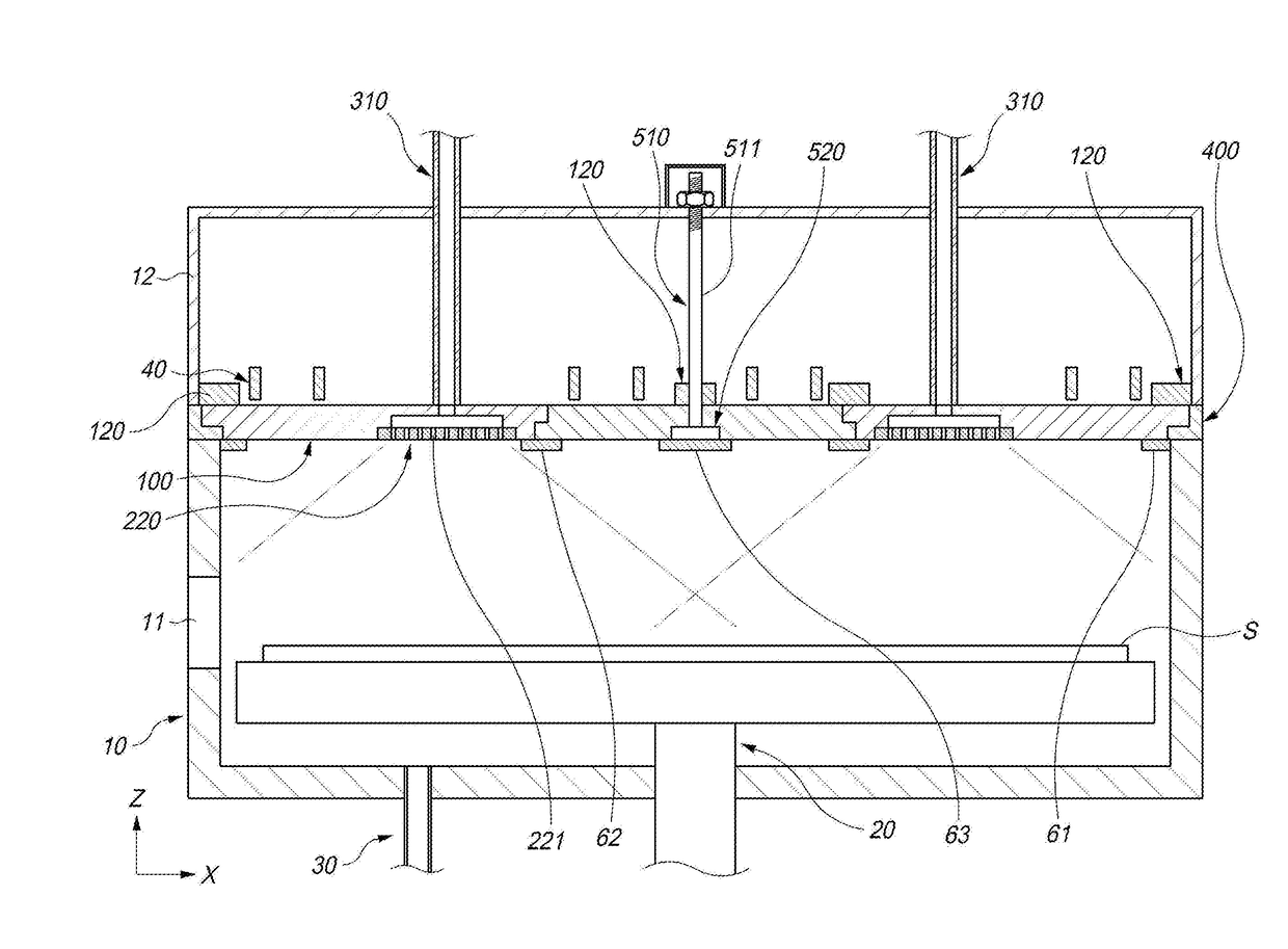
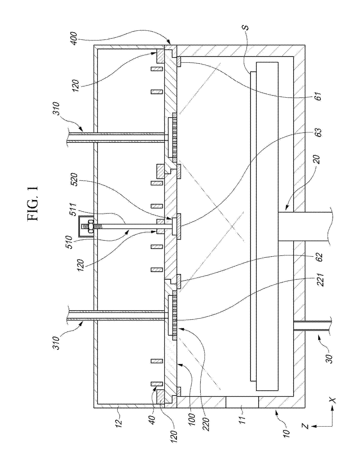
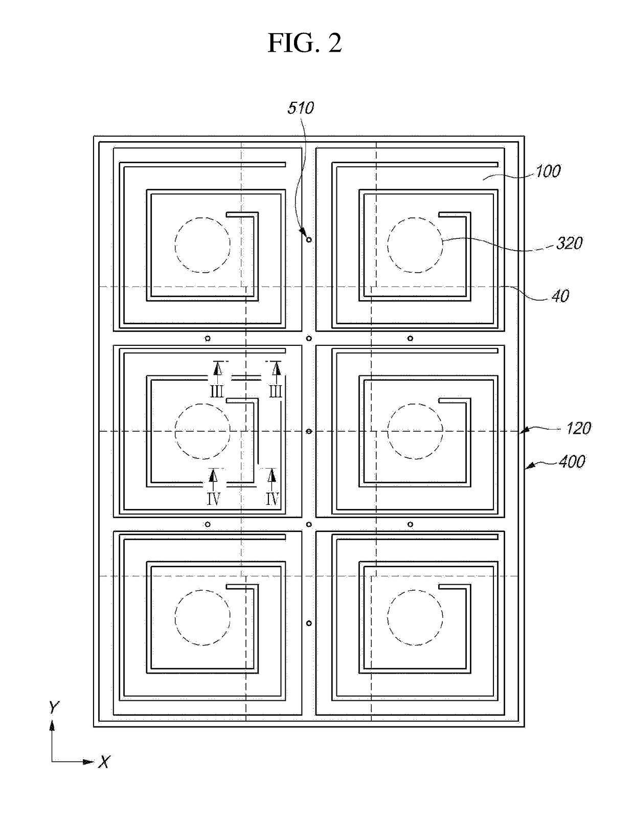
[0032]In the following, an embodiment of the present invention is described with reference to the accompanying drawings. FIG. 1 is a cross-sectional view showing an inductively coupled plasma processing apparatus according to an embodiment of the present invention, FIG. 2 is a plan view showing a dielectric wall and a supporting member in FIG. 1, FIG. 3a is a cross-sectional view taken along line III-III and IV-IV in FIG. 2, FIG. 3b is a cross-sectional view taken along line V-V in FIG. 2, FIG. 3c and FIG. 3d are cross-sectional views of the respective modified example of FIG. 3a and FIG. 3b, FIG. 4a and FIG. 4b are plan views showing a dielectric window supporting unit of FIG. 1, FIG. 5 is a plan view showing an example of an RF antenna that is installed at the apparatus shown in FIG. 1, FIG. 6 is an equivalent circuit diagram of the RF antenna in FIG. 2, FIG. 7 is a plan view showing an example of an arrangement of an RF antenna that is installed at the apparatus shown in FIG. 1, ...


PUM


Abstract

An Dielectric window of an inductively coupled plasma (ICP) processing apparatus that includes a main container 10 that houses a substrate to be processed S to perform plasma processing, a substrate mounting unit 20 on which the substrate to be processed S is mounted in the main container 10, an exhaust system 30 that discharges gas from inside of the main container 10, a dielectric window 100 that form an upper window of the main container 10, and one or more RF antennas 40 which are installed to correspond to the dielectric windows 100 outside the main container 10 and to which RF power is applied to form induced electric field in the main container 10, wherein the dielectric window 100 is formed as one body from one or more dielectric members, and bonded with a ceramic reinforcing member 120 to at least one surface of the upper surface and the lower surface of the dielectric window 100, including a dielectric window supporting unit 500 supporting at least one of the dielectric window 100 and the ceramic reinforcing member 120 by penetrating at least one of the dielectric window 100 and the ceramic reinforcing member 120 and being connected with a supporting member 12 installed above the main container 10, is provided, so it is possible to minimize power loss by the replacement of a dielectric supporting structure at a region where an antenna is installed, with ceramic.

Description

CROSS-REFERENCE TO RELATED APPLICATION[0001]This application claims priority to Korean Patent Application No. 10-2016-0055761 filed on May 11, 2016 and all the benefits accruing therefrom under 35 U.S.C. §119, the contents of which are incorporated by reference in their entirety.BACKGROUND OF THE INVENTION1. Field of the Invention[0002]The present disclosure relates to an inductively coupled plasma processing apparatus that performs substrate processing, such as substrate etching or deposition.2. Background of the Invention[0003]In order to perform predetermined processing on a substrate in the manufacturing process of a liquid crystal display (LCD) or an organic light-emitting diode (OLED), various plasma processing apparatuses such as a plasma etching apparatus or plasma CVD deposition apparatus are used. A capacitively coupled plasma processing apparatus has been typically used as such a plasma processing apparatus, but in recent, an inductively coupled plasma (ICP) processing ap...

Claims


Application Information

Patent Timeline
IPC IPC(8): H01J37/32
CPCH01J37/3211H01J37/32119H01J37/32174
Inventor CHO, SAENG HYUN
Owner APPLIED MATERIALS INC
Why Eureka
Try Eureka