Light-Emitting Element, Light-Emitting Device, Electronic Device, and Lighting Device

a light-emitting element and electronic device technology, applied in the field of light-emitting elements, can solve the problem that the quantum efficiency of the internal light-emitting element for fluorescence and phosphorescence is going to reach the theoretical limit, and achieve the effect of high emission efficiency

Active Publication Date: 2017-11-23
SEMICON ENERGY LAB CO LTD
View PDF5 Cites 9 Cited by
  • Summary
  • Abstract
  • Description
  • Claims
  • Application Information

AI Technical Summary

Benefits of technology

[0012]An object of one embodiment of the present invention is to provide a novel light-emitting element. Another object is to provide a novel light-emitting element with high emission efficiency.

Problems solved by technology

However, the internal quantum efficiency of a light-emitting element for both fluorescence and phosphorescence is going to reach the theoretical limit; in particular, by utilizing a triplet excited state, some light-emitting elements that emit fluorescence have achieved an internal quantum efficiency of 25%, which is a theoretical limit, or higher.

Method used


Image

  • Light-Emitting Element, Light-Emitting Device, Electronic Device, and Lighting Device
  • Light-Emitting Element, Light-Emitting Device, Electronic Device, and Lighting Device
  • Light-Emitting Element, Light-Emitting Device, Electronic Device, and Lighting Device

Examples


example 1

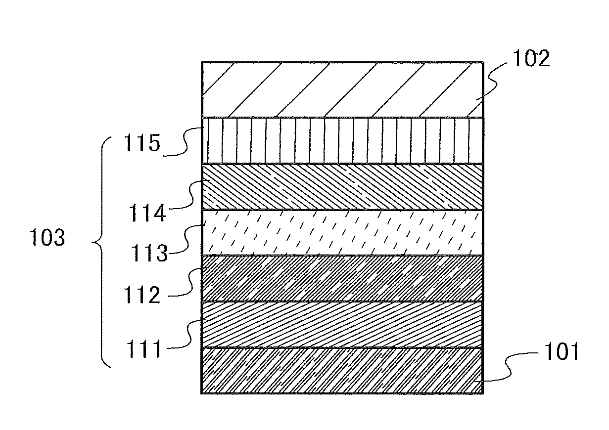
[0256]In this example, results of calculating the parameter a of a light-emitting element (Light-emitting Element 1) of one embodiment of the present invention with high efficiency are described in detail. For the above purpose, a light-emitting element (Light-emitting Element 1-1) for measurement which includes a light-emitting layer having the same structure as that of Light-emitting Element 1 and in which the luminance in the front direction is reduced as much as possible was also fabricated. FIG. 18 illustrates the structure of the light-emitting element.

[0257]First, a fabrication method and the structure of the light-emitting element of one embodiment of the present invention are described. Organic compounds used in the light-emitting element of one embodiment of the present invention are given below.

(Fabrication Method of Light-Emitting Element 1)

[0258]First, a film of indium tin oxide containing silicon oxide (ITSO) was formed over a glass substrate by a sputtering method, so...

example 2

[0277]In this example, results of calculating the parameter a of a light-emitting element (Light-emitting Element 2) of one embodiment of the present invention with high efficiency are described in detail. For the above purpose, a light-emitting element (Light-emitting Element 2-1) for measurement which includes a light-emitting layer having the same structure as that of Light-emitting Element 2 and in which the luminance in the front direction is reduced as much as possible was also fabricated.

[0278]First, a fabrication method and the structure of the light-emitting element of one embodiment of the present invention are described. Organic compounds used in the light-emitting element of one embodiment of the present invention are given below.

(Fabrication Method of Light-Emitting Element 2)

[0279]First, a film of indium tin oxide containing silicon oxide (ITSO) was formed over a glass substrate by a sputtering method, so that the first electrode 101 was formed. The thickness of the fi...

example 3

[0298]In this example, results of calculating the parameter a of a light-emitting element (Light-emitting Element 3) of one embodiment of the present invention with high efficiency are described in detail. For the above purpose, a light-emitting element (Light-emitting Element 3-1) for measurement which includes a light-emitting layer having the same structure as that of Light-emitting Element 3 and in which the luminance in the front direction is reduced as much as possible was also fabricated.

[0299]First, a fabrication method and the structure of the light-emitting element of one embodiment of the present invention are described. Organic compounds used in the light-emitting element of one embodiment of the present invention are given below.

(Fabrication Method of Light-Emitting Element 3)

[0300]First, a film of indium tin oxide containing silicon oxide (ITSO) was formed over a glass substrate by a sputtering method, so that the first electrode 101 was formed. The thickness of the fi...


PUM

PropertyMeasurementUnit
external quantum efficiencyaaaaaaaaaa

Abstract

A light-emitting element is provided. The light-emitting element includes first and second electrodes and an EL layer therebetween. The EL layer includes a light-emitting layer containing first and second substances. The amount of the first substance is larger than that of the second substance. The second substance emits light. Average transition dipole moments of the second substance are divided into three components in x-, y-, and z-directions which are orthogonal to each other. Components parallel to the first or second electrode are assumed to be the components in the x- and y-directions, and a component perpendicular to the first or second electrode is assumed to be the component in the z-direction. The proportion of the component in the z-direction is represented by a, which is less than or equal to 0.2.

Description

BACKGROUND OF THE INVENTION1. Field of the Invention[0001]One embodiment of the present invention relates to a light-emitting element, a display module, a lighting module, a display device, a light-emitting device, an electronic device, and a lighting device. Note that one embodiment of the present invention is not limited to the above technical field. The technical field of one embodiment of the invention disclosed in this specification and the like relates to an object, a method, or a manufacturing method. One embodiment of the present invention relates to a process, a machine, manufacture, or a composition of matter. Specifically, examples of the technical field of one embodiment of the present invention disclosed in this specification include a semiconductor device, a display device, a liquid crystal display device, a light-emitting device, a lighting device, a power storage device, a memory device, a method for driving any of them, and a method for manufacturing any of them.2. ...

Claims


Application Information

Patent Timeline
Patent Type & Authority Applications(United States)
IPC IPC(8): H01L51/50H01L27/32C07D209/82H01L51/00C09K11/06H01L51/56H01L51/52
CPCH01L51/5016H01L27/3258H01L51/56H01L51/0034H01L51/5265H01L27/3244H01L51/52C09K11/06C07D209/82H01L2251/55H01L51/5092H01L51/5246H01L51/5068H01L51/5084H01L51/5215H01L51/5234H01L51/504H01L27/3209H01L51/5262H01L51/0085Y02P20/582H10K85/624H10K85/633H10K85/654H10K85/6576H10K85/342H10K85/6572H10K50/11H10K2101/10H10K2101/90H10K2101/00H10K85/631H10K85/615H10K50/13H10K50/80H10K50/85H10K50/157H10K50/167H10K50/171H10K50/816H10K50/828H10K50/852H10K50/8426H10K59/12H10K59/32H10K59/124H10K71/00H10K85/10
Inventor SEO, SATOSHISEO, HIROMISUZUKI, TSUNENORIKIDO, HIROMITSU
Owner SEMICON ENERGY LAB CO LTD
Why Eureka
Try Eureka