Substrate processing method

Active Publication Date: 2017-11-30
JUSUNG ENG
View PDF6 Cites 0 Cited by
  • Summary
  • Abstract
  • Description
  • Claims
  • Application Information

AI Technical Summary

Benefits of technology

[0016]In the embodiment, deposition films may shrink by repeatedly injecting plasma gas onto the deposition films in surface treatment. Therefore, as the deposition films shrink, the density of the deposition films may be increased. Further, as the deposition films shrink, some of fine air bubbles present within the deposition films or on the surfaces of the deposition films may be removed and uniform

Problems solved by technology

In CVD, since a deposition film is formed on a substrate by injecting process gas for deposition onto the substrate, CVD has high deposition speed but has low uniformity and quality of the deposition film, as compared to atomic layer deposition.
Particularly, if a gap

Method used


Image

  • Substrate processing method
  • Substrate processing method
  • Substrate processing method

Examples


Example

BEST MODE

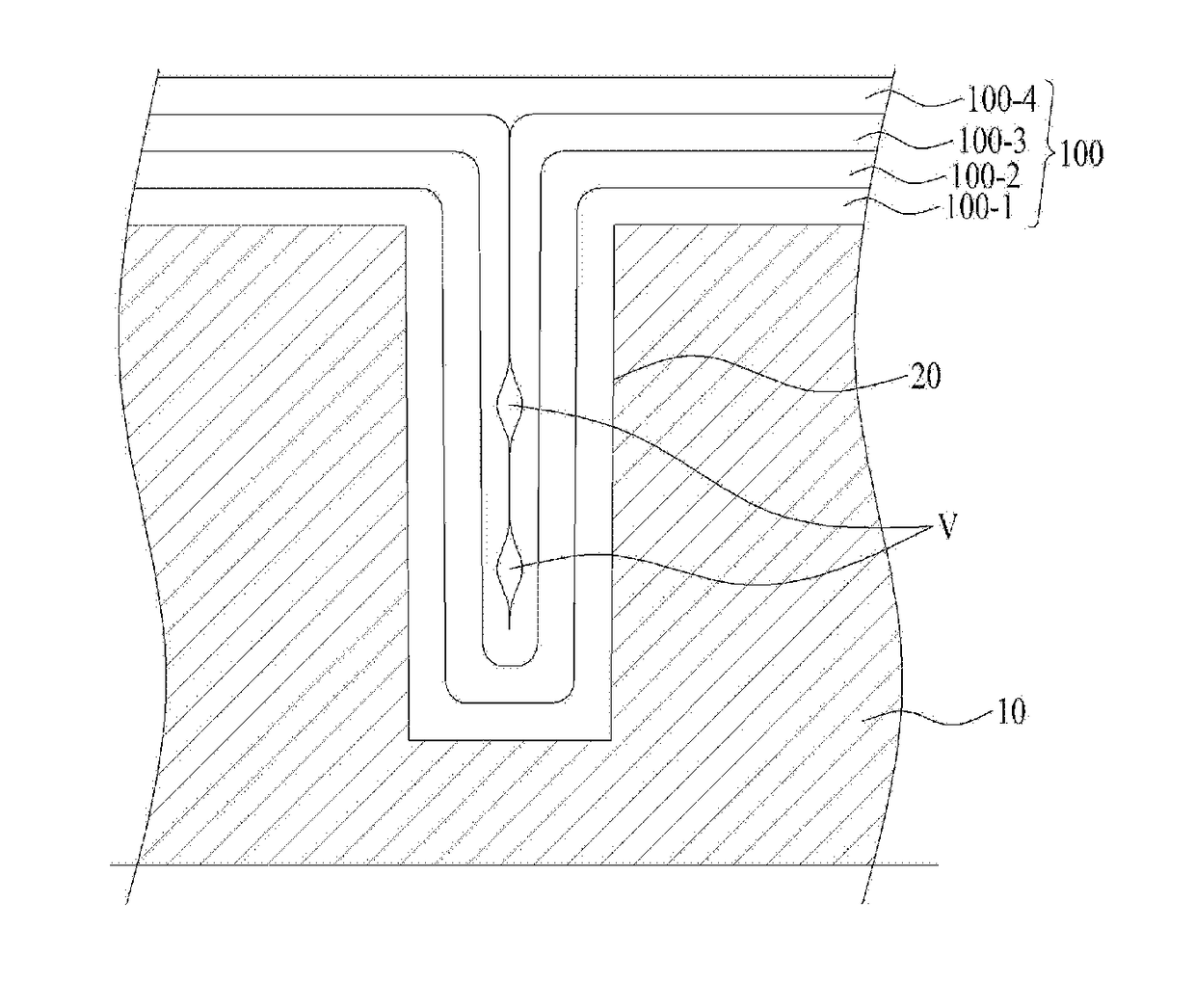
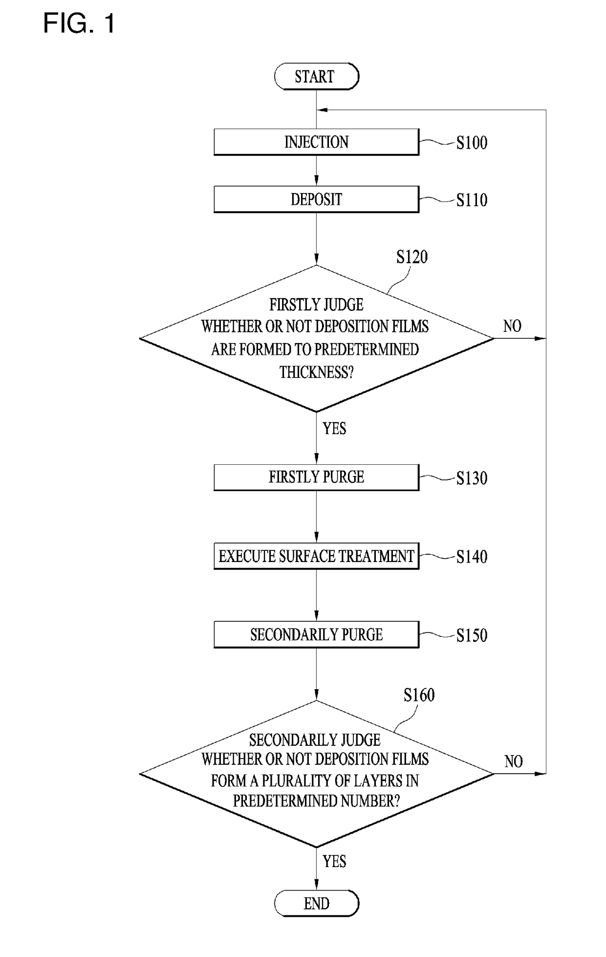
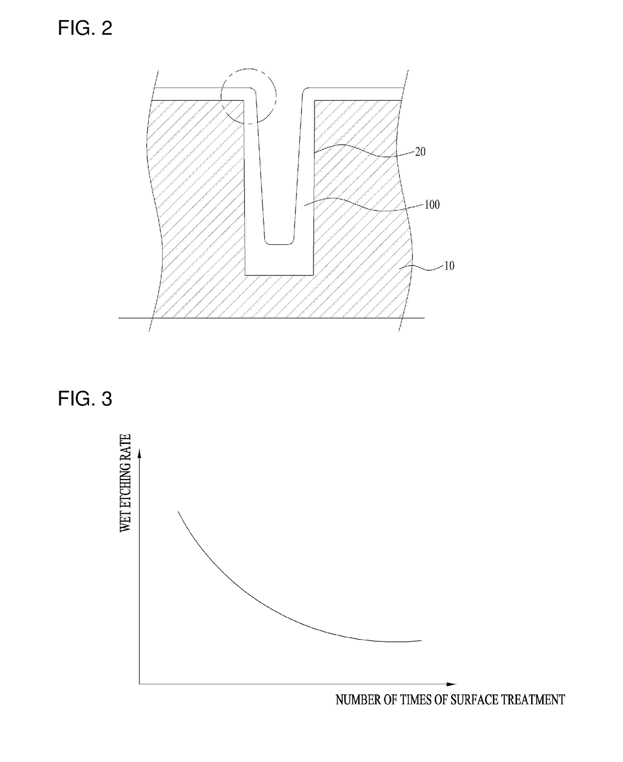
[0024]Hereinafter, embodiments will be described with reference to the annexed drawings. These embodiments may be variously modified but specific embodiments will be exemplarily described with reference to the annexed drawings. However, the embodiments are not limited thereto but may cover all modifications, variations and equivalents within the scope of the embodiments. Here, the sizes or shapes of elements shown in the drawings may be exaggerated for clarity and convenience in description.

[0025]Further, the terms “first”, “second”, etc., may be used to describe various elements but the elements are not limited by these terms. The terms are used only to distinguish one element from other elements. In addition, the terms specifically defined in consideration of the configurations and functions of the embodiments are only to describe the embodiments but do not limit the ranges of the embodiments.

[0026]In the following description of the embodiments, it will be understood tha...


PUM

PropertyMeasurementUnit
Thicknessaaaaaaaaaa
Densityaaaaaaaaaa
Processing propertiesaaaaaaaaaa

Abstract

Disclosed is a substrate processing method including gas injection including a source material containing silicon towards substrates received in a reaction chamber, depositing the source material on the substrates by generating plasma including oxygen radicals so as to form deposition films, and executing surface treatment of the deposition films by injecting plasma gas including oxygen radicals.

Description

TECHNICAL FIELD[0001]Embodiments relate to a substrate processing method in which required density and step coverage may be satisfied and generation of voids may be remarkably reduced.BACKGROUND ART[0002]Contents described herein provide only background information of embodiments but do not constitute prior art.[0003]In general, a semiconductor memory device, a liquid crystal display device, an organic light emitting device, etc. are fabricated by depositing and stacking structures of a desired shape by repeating a semiconductor process on a substrate a plurality of times.[0004]Semiconductor fabrication includes a process of a depositing a designated thin film on a substrate, a photolithography process for exposing selected regions of the thin film, an etching process for removing the thin film from the selected regions, etc. Such semiconductor fabrication is carried out within a reaction chamber in which optimal conductions for the corresponding process are realized.[0005]The subst...

Claims


Application Information

Patent Timeline
IPC IPC(8): H01L21/02H01J37/32
CPCH01L21/02274H01L21/02164H01J37/3244H01L21/0228C23C16/402C23C16/4408C23C16/52C23C16/56H01L21/205H01L21/2053H01L21/2056
Inventor SHIN, SEUNG CHULYOO, JIN HYUKCHEON, MIN HOHWANG, CHUL-JOO
Owner JUSUNG ENG
Why Eureka
Try Eureka