Antenna and electronic device including the same

a technology of electronic devices and antennas, applied in the field of electronic devices, can solve the problems of loss of efficiency (rx performance) of antennas, excessive antenna design for supporting cellular networks, and insufficient loading space of electronic devices such as smartphones or tablets

Active Publication Date: 2017-12-21
SAMSUNG ELECTRONICS CO LTD
View PDF7 Cites 30 Cited by
  • Summary
  • Abstract
  • Description
  • Claims
  • Application Information

AI Technical Summary

Benefits of technology

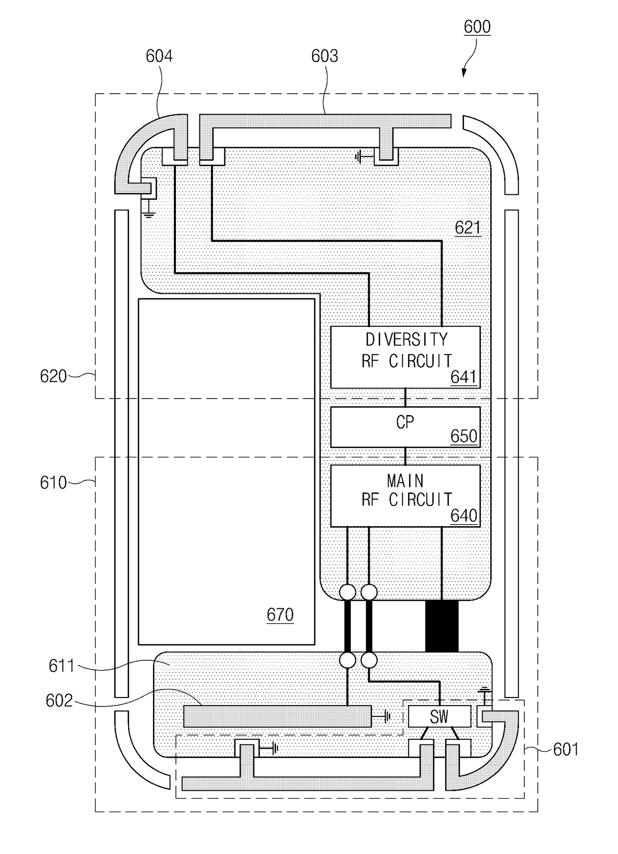
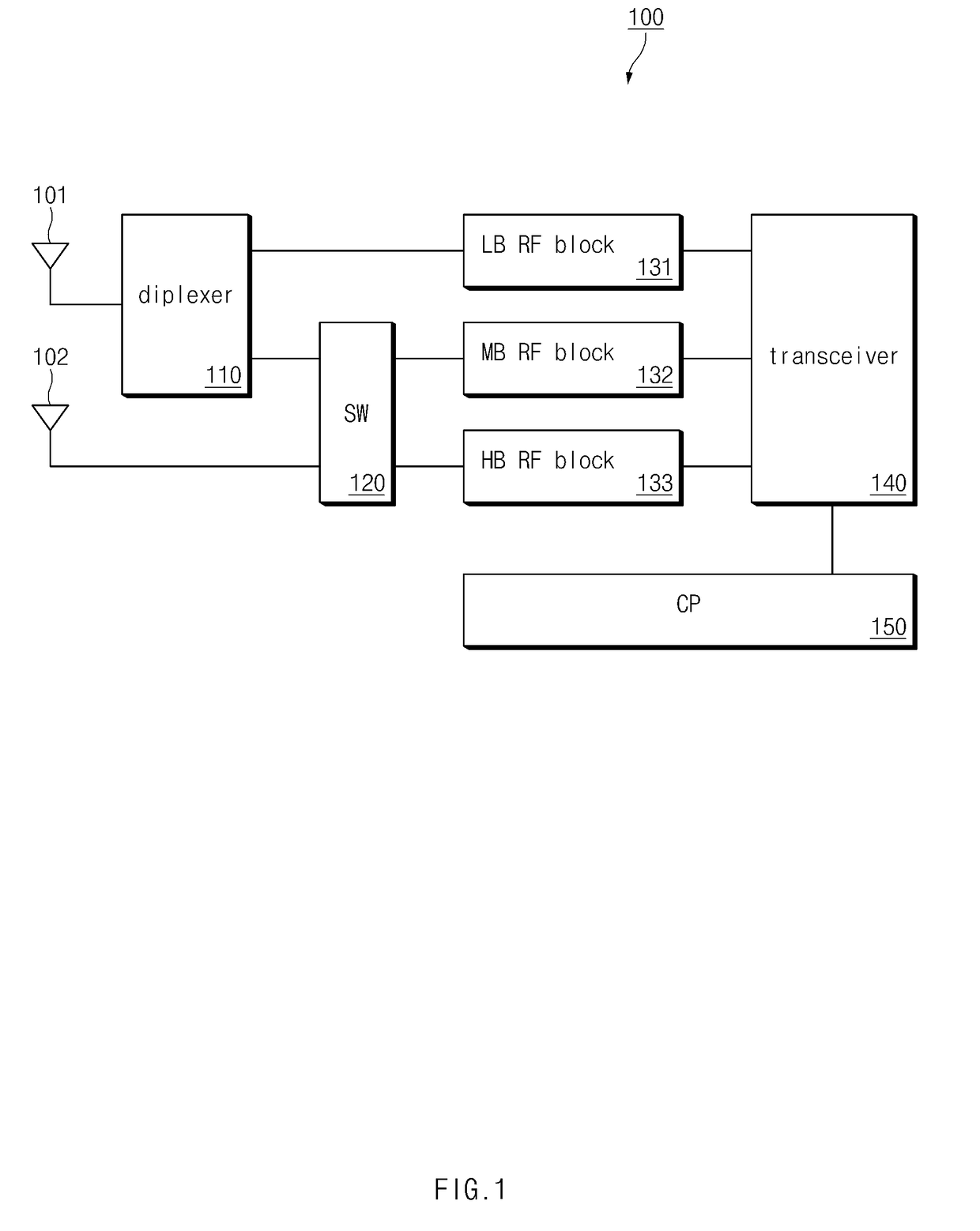
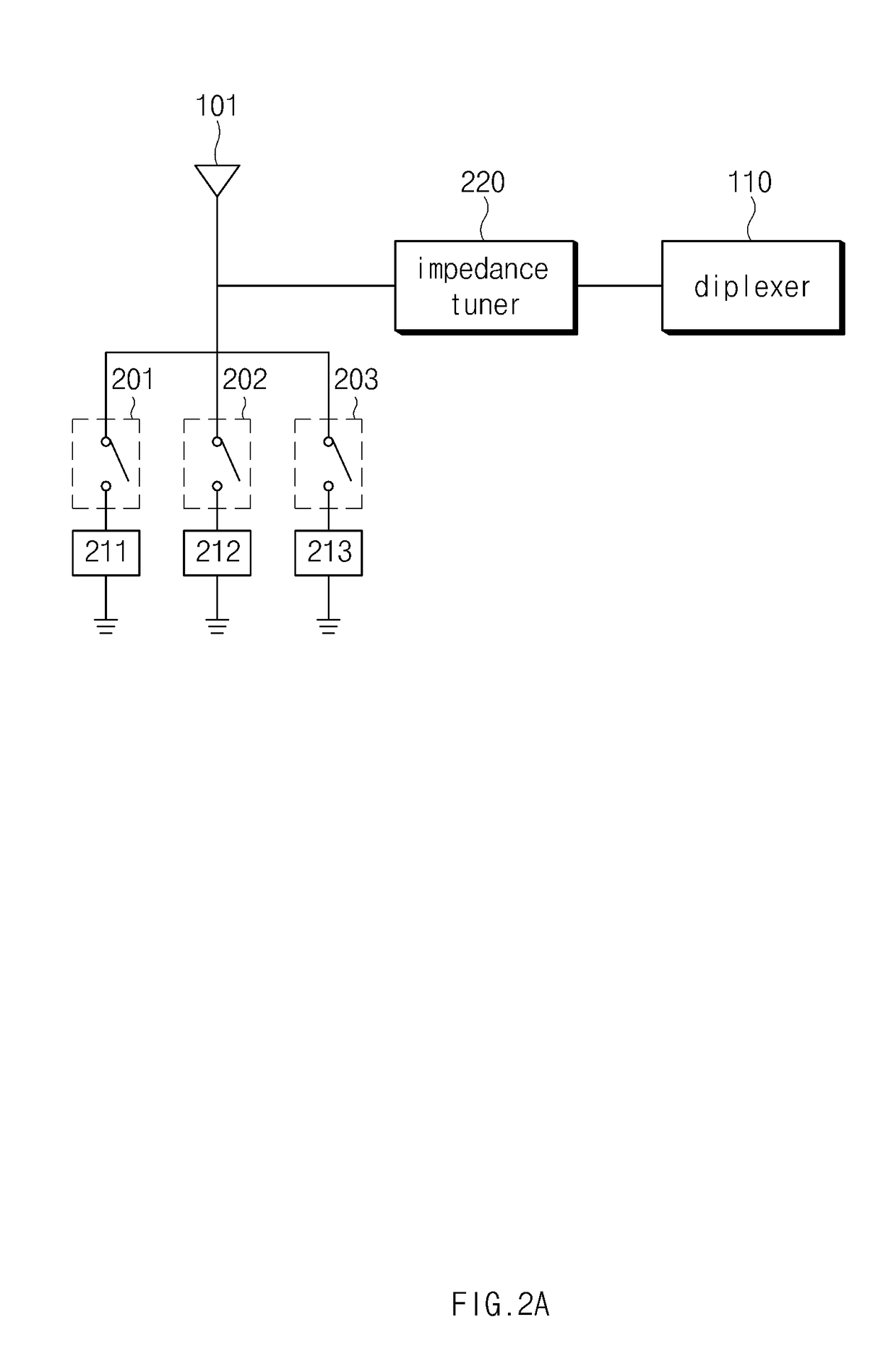
[0013]In accordance with another aspect of the present disclosure, an electronic device includes a first antenna element, a first switch configured to enable the first antenna element to receive a signal of a first frequency band and a second frequency or receive a signal of the first frequency band and a third frequency band, a second antenna element configured to receive a signal of the third frequency band, a first RF block configured to process a signal of the first frequency band, a second RF block configured to process a signal of the second frequency band, a third RF block configured to process the signal of the third frequency band, a second switch configured to connect the first antenna element with the second RF block or the third RF block according to a connection of th

Problems solved by technology

However, an electronic device such as a smartphone or a tablet may have a loading space insufficient to load each of antennas for communicating with frequency bands.
Since antennas such as coils for a global positioning system (GPS), Bluetooth®, wireless fidelity (Wi-Fi), near field communication (NFC), or magnetic stripe transmission (MST), wireless charging other than an LTE network are loaded into each of electronic devices, causing an excessive antenna design for supporting the cellular network.
Thus, a general antenna radiator may be designed to cover a low band (LB) and a mid-band (MB) together and/or cover an LB and an (HB) together, although some loss occurs in efficiency (Rx performance) of the antenna.
In another example, a radiator which covers all of an LB, MB,

Method used


Image

  • Antenna and electronic device including the same
  • Antenna and electronic device including the same
  • Antenna and electronic device including the same

Examples


Embodiment Construction

[0028]Embodiments of the present disclosure will be described with reference to accompanying drawings. Accordingly, those of ordinary skill in the art will recognize that modification, equivalent, and / or alternative on the embodiments described herein can be made without departing from the scope and spirit of the present disclosure. With regard to description of drawings, similar elements may be marked by similar reference numerals.

[0029]In this disclosure, the expressions “have”, “may have”, “include” and “comprise”, or “may include” and “may comprise” indicate the existence of corresponding features, such as numeric values, functions, operations, or components, but do not exclude presence of additional features.

[0030]In this disclosure, the expressions “A or B”, “at least one of A or / and B”, or “one or more of A or / and B” may include any and all combinations of one or more of the associated listed items. For example, the expression “A or B”, “at least one of A and B”, or “at least...


PUM


Abstract

Disclosed is an electronic device including a first antenna element configured selectively to receive signals of a first frequency band and a second frequency band or of the first frequency band and a third frequency band, a second antenna element configured to receive a signal of the third frequency band, a transceiver configured to be electrically connected with the first antenna element and the second antenna element, and a processor configured to be electrically connected with the transceiver. The electronic device performs carrier aggregation using the second frequency band and the third frequency band.

Description

PRIORITY[0001]This application claims priority under 35 U.S.C. §119(a) to a Korean Patent Application filed in the Korean Intellectual Property Office on Jun. 16, 2016 and assigned Serial Number 10-2016-0075156, the contents of which are incorporated herein by reference.BACKGROUND1. Field of the Disclosure[0002]The present disclosure relates generally to an electronic device, and more particularly, to technologies for performing carrier aggregation (CA) using a plurality of antennas included in an electronic device.2. Description of the Related Art[0003]An electronic device such as a smartphone or a tablet may communicate with a network using an antenna. Contrary to 3rd generation partnership project (3G) in which a few frequency bands, such as 900 MHz, 1.8 GHz, or 2.1 GHz are globally used, a long term evolution (LTE) or LTE-advanced (LTE-A) network proceeding 3G may use a variety of frequency bands for each country and / or each mobile network operator (MNO).[0004]According to Table...

Claims


Application Information

Patent Timeline
IPC IPC(8): H01Q1/24H04B7/08H01Q5/50H01Q1/38H04L5/14H04B7/12
CPCH01Q1/243H01Q5/50H04B7/0805H04L5/14H04B7/12H01Q1/38H01Q3/24H01Q9/42H01Q21/28H04B7/0602H04B7/0802H04B1/0064H04B1/0053H04B7/0871H01Q21/30H01Q5/335
Inventor HONG, SANG HOSON, MU CHANGPARK, SUNG CHUL
Owner SAMSUNG ELECTRONICS CO LTD
Why Eureka
Try Eureka