
Ultrasonic fingerprint recognition module and manufacturing method thereof
- Summary
- Abstract
- Description
- Claims
- Application Information
AI Technical Summary
Benefits of technology
Problems solved by technology
Method used
Image

Examples
Embodiment Construction
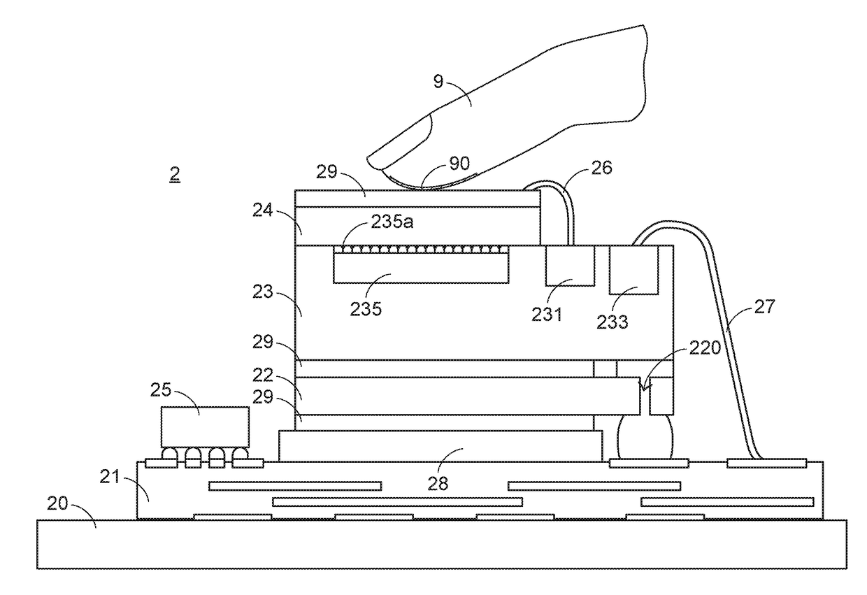
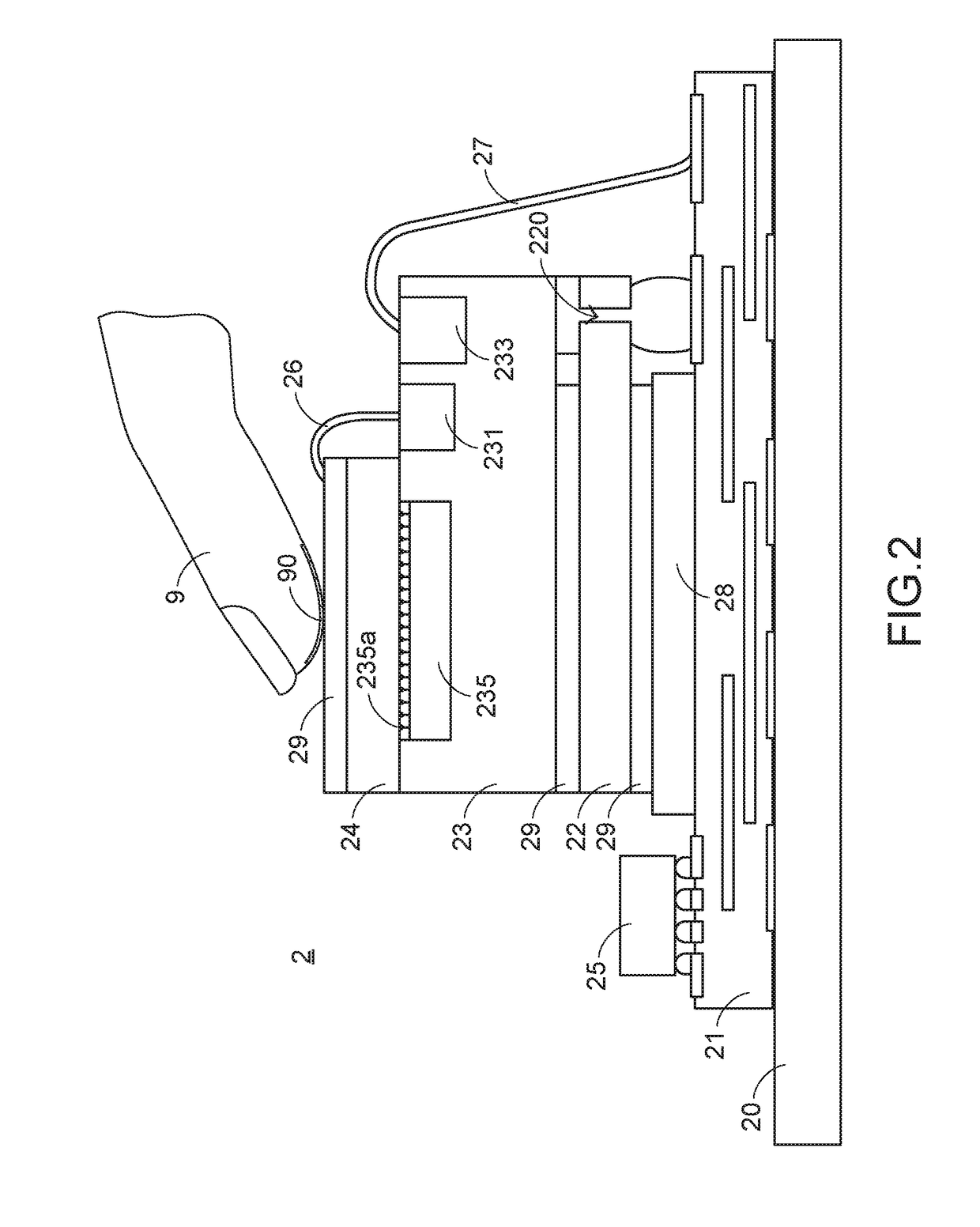
[0029]FIG. 2 is a schematic cross-sectional view illustrating an ultrasonic fingerprint recognition module according to a first embodiment of the present invention. As shown in FIG. 2, the ultrasonic fingerprint recognition module 2 comprises a substrate 21, an ultrasonic transmitter 22, a thin film transistor (TFT) 23, an ultrasonic receiver 24, a first wire 26 and a second wire 27. The above components will be described according to the sequence from bottom to top.
[0030]The substrate 21 is located at a bottom side. The ultrasonic transmitter 22 is stacked over the substrate 21. The thin film transistor 23 is stacked over the ultrasonic transmitter 22. The ultrasonic receiver 24 is stacked over the thin film transistor 23. The two ends of the first wire 26 are connected with the ultrasonic receiver 24 and a first electric pad 231 of the thin film transistor 23, respectively. Consequently, the ultrasonic receiver 24 and the thin film transistor 23 are electrically connected with eac...
PUM
 Abstract
Description
Claims
Application Information