Manufacturing method of semiconductor device

a manufacturing method and semiconductor technology, applied in semiconductor devices, semiconductor/solid-state device details, electrical devices, etc., can solve the problems of deteriorating the operational reliability of the semiconductor device, and affecting the operation of the device. achieve the effect of improving the operational reliability

Active Publication Date: 2018-01-04
SK HYNIX INC
View PDF0 Cites 38 Cited by
  • Summary
  • Abstract
  • Description
  • Claims
  • Application Information

AI Technical Summary

Benefits of technology

[0006]Various embodiments of the present invention are directed to a manufacturing method of a 3D semiconductor device having improved operational reliability.

Problems solved by technology

As the number of stacked memory cell increases, connecting the channel layer with the source layer becomes more difficult and current supply to the cells may suffer.
As a result, the operational reliability of the semiconductor device may be deteriorated due to a decrease in cell current.

Method used


Image

  • Manufacturing method of semiconductor device
  • Manufacturing method of semiconductor device
  • Manufacturing method of semiconductor device

Examples


Embodiment Construction

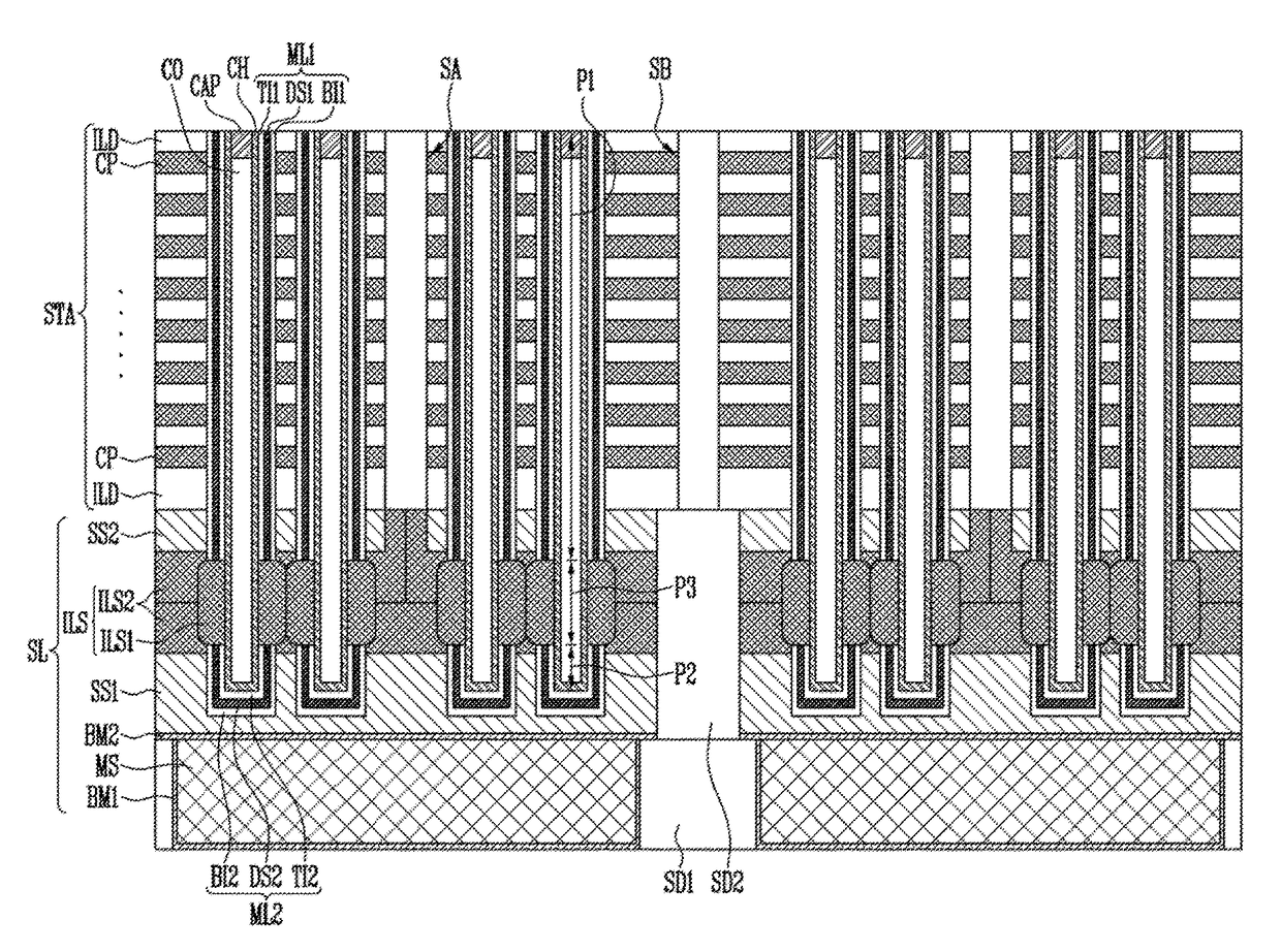
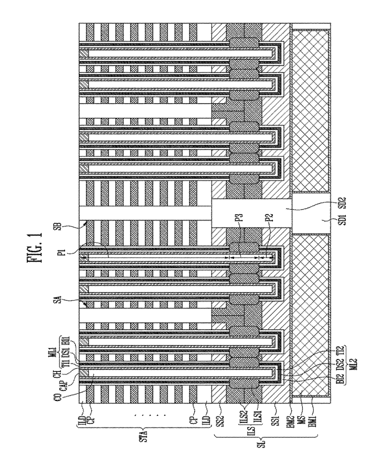
[0013]Example embodiments of the present disclosure will be described with reference to the accompanying drawings. The example embodiments of the present disclosure may, however, be embodied in many different forms and should not be construed as being limited only to the example embodiments set forth herein. Rather, the example embodiments are provided so that disclosure of the present disclosure will be thorough and complete, and will fully convey the present disclosure to those skilled in the art to which the present invention pertains. The features of example embodiments of the present disclosure may be employed in various and numerous embodiments without departing from the scope of the present disclosure. In the drawings, the size and relative sizes of layers and areas may be exaggerated for clarity. The drawings are not to scale. Like reference numerals refer to like elements throughout. In the drawing figures, dimensions may be exaggerated for clarity of Illustration. It will ...


PUM


Abstract

There are provided a manufacturing method of a semiconductor device. A manufacturing method of a semiconductor device includes forming a preliminary source stack structure including a first source layer, a first protective layer, a sacrificial layer, a second protective layer, and a second source layer, which are sequentially stacked in the recited order, forming channel layers extending through the second source layer and partially inside the first source layer, and growing a first region of an interlayer source layer from each channel layer, the first region of the interlayer source layer surrounding each channel layer in a region between the first and second protective layers.

Description

CROSS-REFERENCE TO RELATED APPLICATION[0001]The present application claims priority under 35 U.S.C. §119(a) to Korean patent application no. 10-2016-0082711, filed on Jun. 30, 2016, which is incorporated herein by reference in its entirety.BACKGROUND1. Field[0002]An aspect of the present disclosure relates to a manufacturing method of a semiconductor device, and more particularly, to a manufacturing method of a three-dimensional semiconductor memory device.2. Description of the Related Art[0003]A semiconductor device typically includes a plurality of memory cells capable of storing data. A three-dimensional semiconductor memory device including three-dimensionally arranged memory cells has been proposed in order to achieve a high degree of integration of semiconductor devices.[0004]The memory cells of a three-dimensional semiconductor memory device may be stacked over each other. The memory cells may be connected in series in units of memory strings through a channel layer. The chan...

Claims


Application Information

Patent Timeline
Patent Type & Authority Applications(United States)
IPC IPC(8): H01L27/11582H01L21/768H01L23/528
CPCH01L27/11582H01L21/76843H01L21/76879H01L23/5283H10B43/27H10B41/20H10B41/30H10B43/20H10B41/27H10B43/30
Inventor HWANG, SUN KAK
Owner SK HYNIX INC
Why Eureka
Try Eureka