Nitride Semiconductor Light Emitting Device and Fabrication Method Thereof

a technology of nitride semiconductor and light emitting device, which is applied in the direction of semiconductor/solid-state device manufacturing, semiconductor devices, semiconductor devices, etc., can solve the problems of affecting the gan layer is grown in the trench, and the reliability of the light emitting device is affected, so as to improve the efficiency of optical extraction and operational reliability of the nitride semiconductor light emitting device, improve the luminous efficiency, and improve the utilization

Inactive Publication Date: 2009-07-02
LG INNOTEK CO LTD
View PDF30 Cites 30 Cited by
  • Summary
  • Abstract
  • Description
  • Claims
  • Application Information

AI Technical Summary

Benefits of technology

[0019]According to the present invention, the optical extraction efficiency and operational reliability of a nitride semiconductor light emitting device can be improved.
[0020]Also, the light that may be lost is reflected and thus the utilization of light increases, thereby improving the luminous efficiency. Also, crystal defect caused by a patterned portion of a substrate is suppressed, thereby much improving the operational reliability of the light emitting device.

Problems solved by technology

In the interface with the GaN layer grown in the surface, a large amount of treading dislocation (TD) is densely gathered, resulting in degradation in the reliability of the light emitting device.
Although the crystal defect density is determined by the surface roughness of the trench, the depth and the patterned shape, much crystal defect exists in the GaN layer grown within the trench.
Consequently, the crystal defect greatly influences the reliability of the light emitting device.
Consequently, the crystal defect density causes the leakage current in the nitride semiconductor light emitting device and thus badly influences the reliability such as the optical power and life time in long-term operation.

Method used


Image

  • Nitride Semiconductor Light Emitting Device and Fabrication Method Thereof
  • Nitride Semiconductor Light Emitting Device and Fabrication Method Thereof
  • Nitride Semiconductor Light Emitting Device and Fabrication Method Thereof

Examples


embodiment 1

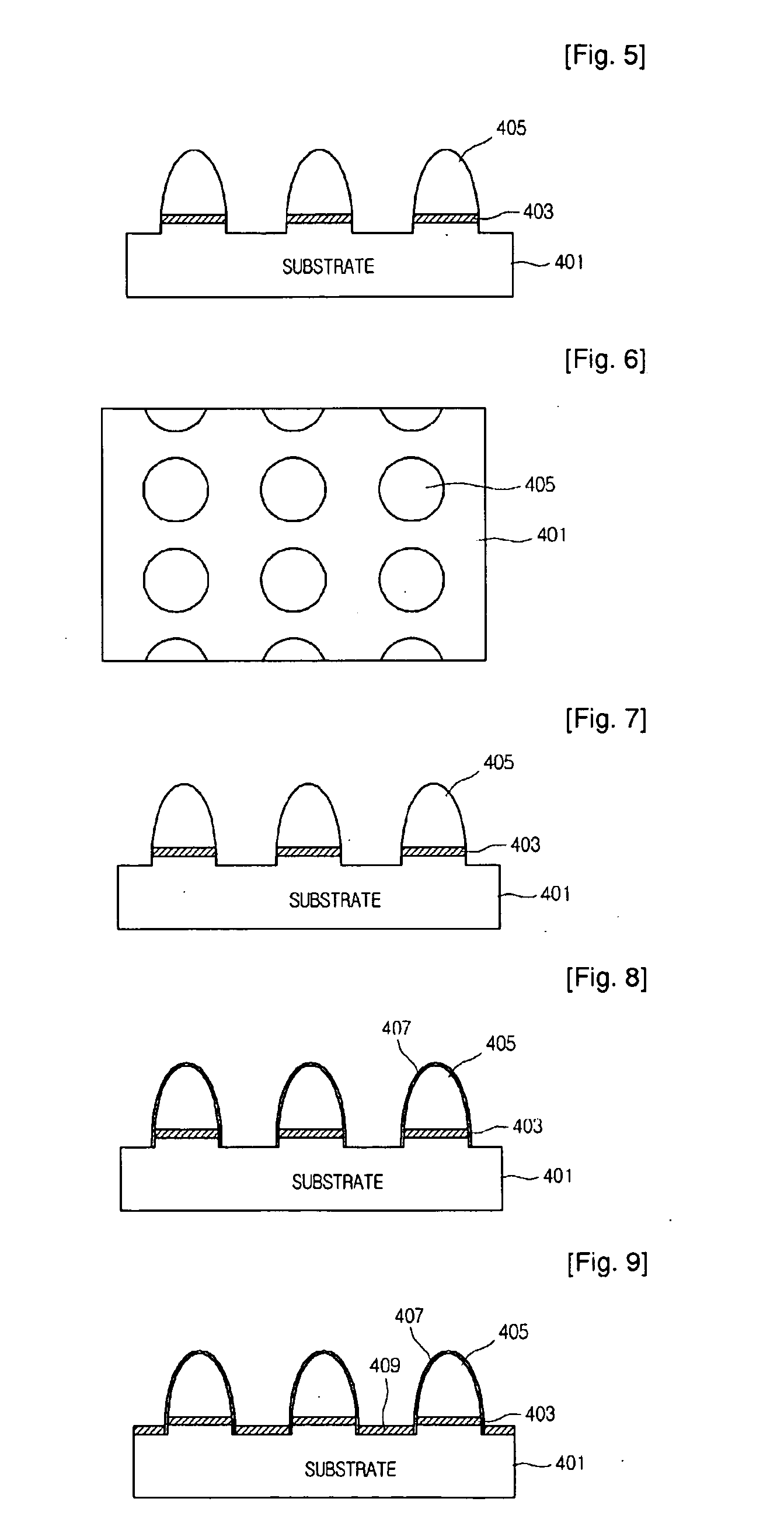
[0033]FIGS. 4 to 6 are views illustrating a method of fabricating a selective etched GaN and sapphire substrate (SEGSS) structure in a nitride semiconductor light emitting device according to the present invention.

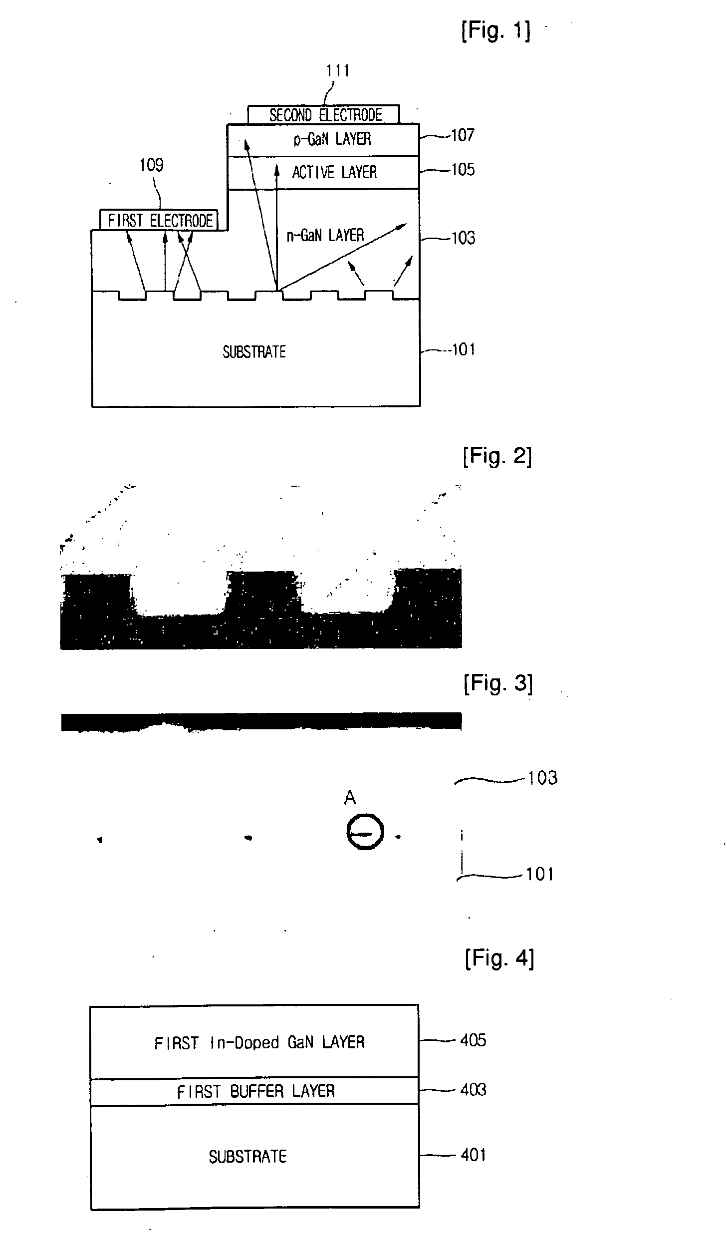
[0034]In order to fabricate an SEGSS substrate of the present invention, a first layer 403 and a first In-doped GaN layer 405 are sequentially formed on a substrate 401, resulting in a staked structure as illustrated in FIG. 4.

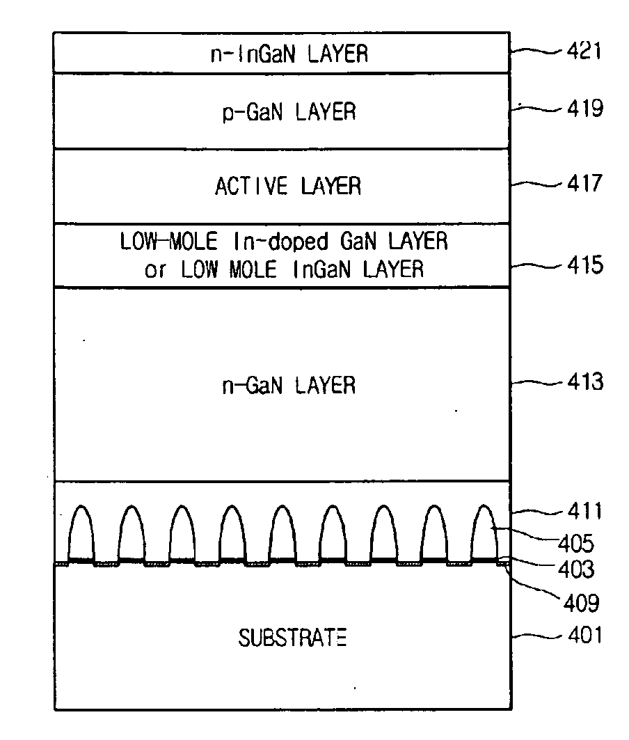
[0035]The substrate 401 may be a sapphire substrate, a silicon carbide substrate, a silicon substrate, or a GaAs substrate. The first buffer layer 403 may be a stack structure of AlInN / GaN, a supper lattice structure of InGaN / GaN, a stack structure of InxGa1−x N / GaN, or a stack structure of AlxInYGa1−(x+Y)N / InxGa1−xN / GaN. Although FIG. 4 illustrates an In-doped GaN layer 405 as the GaN layer formed on the first buffer layer 403, the GaN layer 405 can also be an undoped-GaN layer or a GaN layer formed by doping other material. For example, the doping ...

embodiment 2

[0064]FIGS. 11 and 12 are views illustrating a method of fabricating a nitride semiconductor light emitting device according to a second embodiment of the present invention. FIG. 13 is a sectional view of the nitride semiconductor light emitting device according to the second embodiment of the present invention.

[0065]Referring to FIGS. 11, 12 and 13, the second embodiment is similar to the first embodiment, except that the process of patterning the insulation layer 407 on the first In-doped GaN layer 405 is omitted. Therefore, the difference only will be described.

[0066]According to the second embodiment of the present invention, a secondary GaN layer is re-grown on the SEGSS structure, without performing the process of patterning the SiO2 insulation layer. The secondary GaN growth is performed in a state that the etched corn-shaped GaN layer and the surface of the etched sapphire substrate are exposed.

[0067]In the secondary re-growth of the GaN layer, due to the strain change cause...


PUM


Abstract

The present invention relates to a nitride semiconductor light emitting device including: a substrate having a predetermined pattern formed on a surface thereof by an etch; a protruded portion disposed on a non-etched region of the substrate, and having a first buffer layer and a first nitride semiconductor layer stacked thereon; a second buffer layer formed on the etched region of the substrate; a second nitride semiconductor layer formed on the second buffer layer and the protruded portion; a third nitride semiconductor layer formed on the second nitride semiconductor layer; an active layer formed on the third nitride semiconductor layer to emit light; and a fourth nitride semiconductor layer formed on the active layer. According to the present invention, the optical extraction efficiency of the nitride semiconductor light emitting device can be enhanced.

Description

TECHNICAL FIELD[0001]The present invention is relative to a nitride semiconductor light emitting device and fabrication method thereof, and to a nitride semiconductor light emitting device and a fabrication method thereof that can enhance the optical extraction efficiency.BACKGROUND ART[0002]In order to increase the optical extraction efficiency of a nitride semiconductor light emitting device, a nitride semiconductor layer is grown on a patterned substrate.[0003]In a related art method of fabricating a nitride semiconductor light emitting device, a sapphire substrate or a silicon carbide (SiC) substrate is selectively patterned in a predetermined shape by using a mask material. An exposed portion of the substrate is selectively dry etched. The mask material is then removed to thereby obtain a substrate with a predetermined pattern. A nitride semiconductor layer is grown on the patterned substrate.[0004]FIG. 1 illustrates a stack structure of a related art nitride semiconductor ligh...

Claims


Application Information

Patent Timeline
Patent Type & Authority Applications(United States)
IPC IPC(8): H01L33/00H01L21/20H01L33/06H01L33/10H01L33/12H01L33/32H01L33/42H01L33/44
CPCH01L33/12H01L33/007
Inventor LEE, SUK HUN
Owner LG INNOTEK CO LTD
Why Eureka
Try Eureka