Gate length controlled vertical fets

a technology of vertical fets and gate lengths, which is applied in the direction of basic electric elements, electrical equipment, semiconductor devices, etc., can solve the problems of finned epitaxy having such problems, type of process flow posing defectivity risk, and limited improvements in the manufacture of such devices

Active Publication Date: 2018-01-11
IBM CORP
View PDF2 Cites 61 Cited by
  • Summary
  • Abstract
  • Description
  • Claims
  • Application Information

AI Technical Summary

Problems solved by technology

VFETs (Vertical Field-Effect Transistor) are a promising architecture for beyond 7 nm CMOS (Complementary metal-oxide-semiconductor) technology, but the manufacture of such devices has made limited improvements.
This type of process flow poses a defectivity risk for the finned epitaxy, at the interface between the finned epitaxy region and the bottom source / drain region upon which this epitaxy is grown.
The grown fin has such problems and others.
Such techniques also require additional gate etching (which would compromise gate resistance), but this approach poses a risk for defective epitaxial growth for the finned channel regions.
Additionally, this type of approach requires added complexity in order to form thick gate dielectric and thin gate dielectric devices on the same chip.
In addition, gate length control is very important but difficult in vertical FETs and so there is a need to have a technique that can efficiently control a gate length in vertical FETs.

Method used


Image

  • Gate length controlled vertical fets
  • Gate length controlled vertical fets
  • Gate length controlled vertical fets

Examples


Embodiment Construction

[0032]The invention will now be described with reference to the drawing figures, in which like reference numerals refer to like parts throughout. It is emphasized that, according to common practice, the various features of the drawing are not necessary to scale. On the contrary, the dimensions of the various features can be arbitrarily expanded or reduced for clarity. Exemplary embodiments are provided below for illustration purposes and do not limit the claims.

[0033]Gate length control is very important in vertical FETs. In the present invention, the location of metal gate top is defined by the hard mask used for fin formation such that it is not relevant to gate recess.

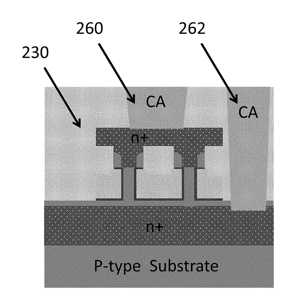
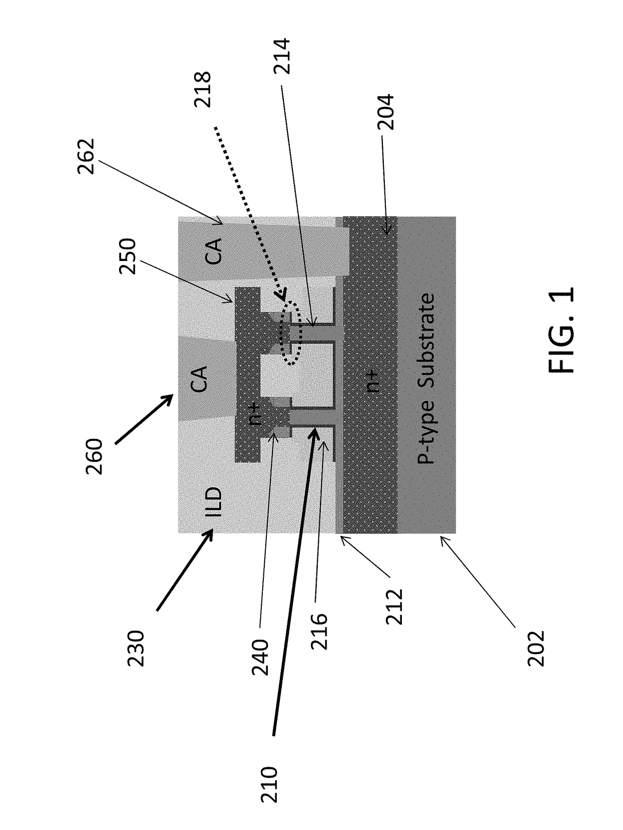
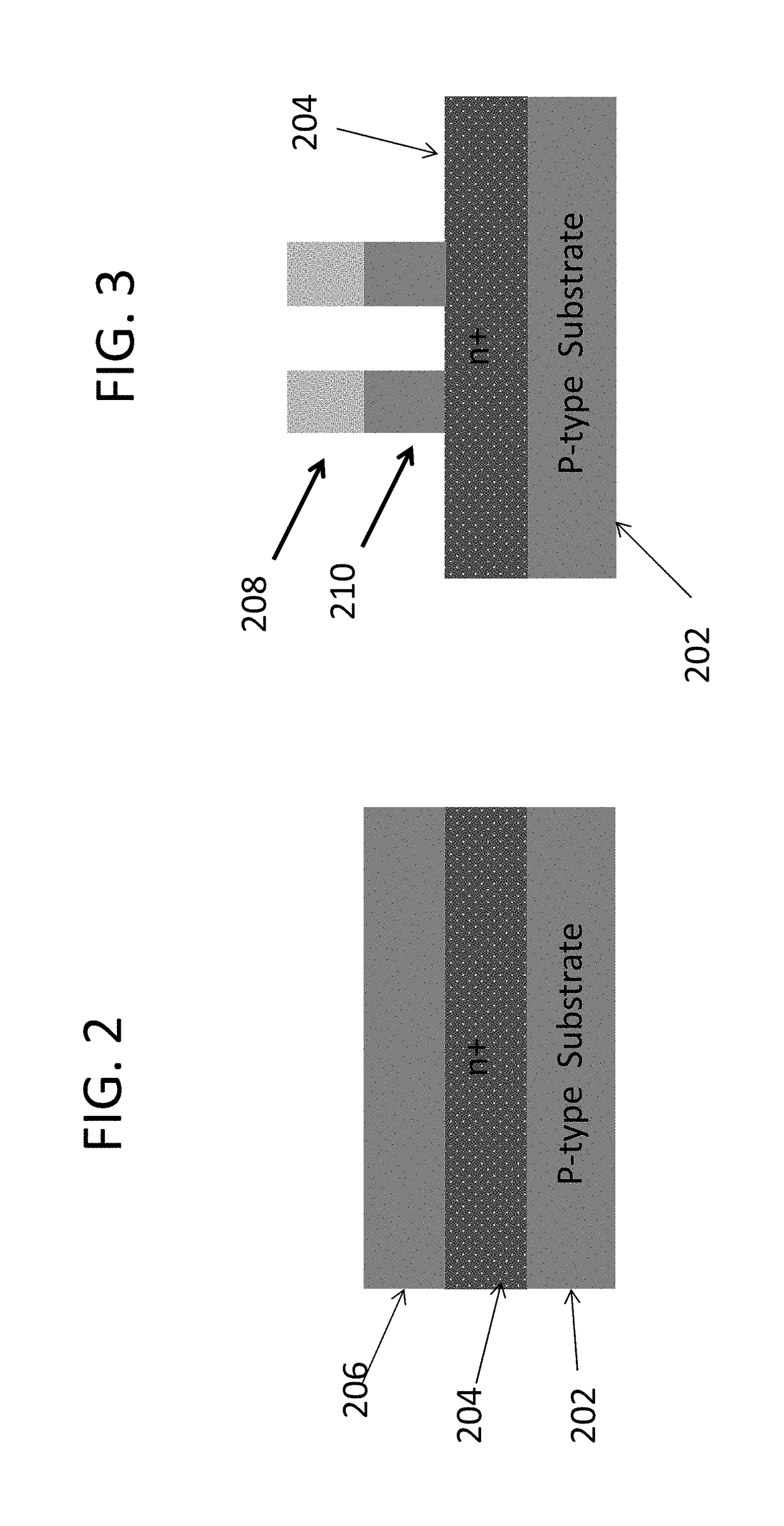
[0034]FIG. 1 illustrates a final VFET structure in an example embodiment. As shown, a p-type (or n-type) substrate 202 is used with a heavily doped n+ (or p+) bottom source-drain layer 204. The bottom space 212 is formed above the bottom source-drain layer 204. The fins 210 are formed above the bottom source-drain 2...


PUM


Abstract

A semiconductor structure and a method a method of forming a vertical FET (Field-Effect Transistor), includes growing a bottom source-drain layer of a second type on a substrate of a first type, growing a channel layer on the bottom source-drain layer, forming a first fin from the channel layer with mask on top of the first fin. A width of the mask is wider than a final first fin width.

Description

BACKGROUND OF THE INVENTIONField of the Invention[0001]The present invention relates generally to a method and apparatus for Vertical FETs (Field-Effect Transistors), and more particularly, but not by way of limitation, relating to a method and apparatus for gate length controlled vertical FETs.Description of the Related Art[0002]VFETs (Vertical Field-Effect Transistor) are a promising architecture for beyond 7 nm CMOS (Complementary metal-oxide-semiconductor) technology, but the manufacture of such devices has made limited improvements. Some integration techniques require the finned channel region to be formed by growth inside a confined cavity. Such VFET integration schemes assume that the fin region is formed inside such a cavity, which is defined / etched through the material that eventually becomes the bottom source / drain spacer. This type of process flow poses a defectivity risk for the finned epitaxy, at the interface between the finned epitaxy region and the bottom source / drai...

Claims


Application Information

Patent Timeline
Patent Type & Authority Applications(United States)
IPC IPC(8): H01L29/78H01L29/10H01L21/8234H01L21/02H01L21/3105H01L21/033H01L29/66H01L29/08
CPCH01L29/7827H01L29/66666H01L21/31055H01L29/1037H01L29/0847H01L21/0332H01L21/823487H01L21/02636
Inventor CHENG, KANGGUOMIAO, XINXU, WENYUZHANG, CHEN
Owner IBM CORP
Why Eureka
Try Eureka