
Three-dimensional semiconductor device and method of fabrication

a semiconductor device and three-dimensional technology, applied in the direction of semiconductor devices, electrical devices, transistors, etc., can solve the problems of accelerating efforts that are facing greater challenges

Active Publication Date: 2018-01-25
TOKYO ELECTRON LTD
View PDF1 Cites 28 Cited by
  • Summary
  • Abstract
  • Description
  • Claims
  • Application Information

AI Technical Summary

Benefits of technology

This patent describes a semiconductor device with a unique structure that allows for the independent connection of each nanowire in the device. This may provide better performance and reliability.

Problems solved by technology

Scaling efforts have greatly increased the number of transistors per unit area in 2D circuits, yet scaling efforts are running into greater challenges as scaling enters single digit nanometer semiconductor device fabrication nodes.

Method used


Image

  • Three-dimensional semiconductor device and method of fabrication
  • Three-dimensional semiconductor device and method of fabrication
  • Three-dimensional semiconductor device and method of fabrication

Examples


Embodiment Construction

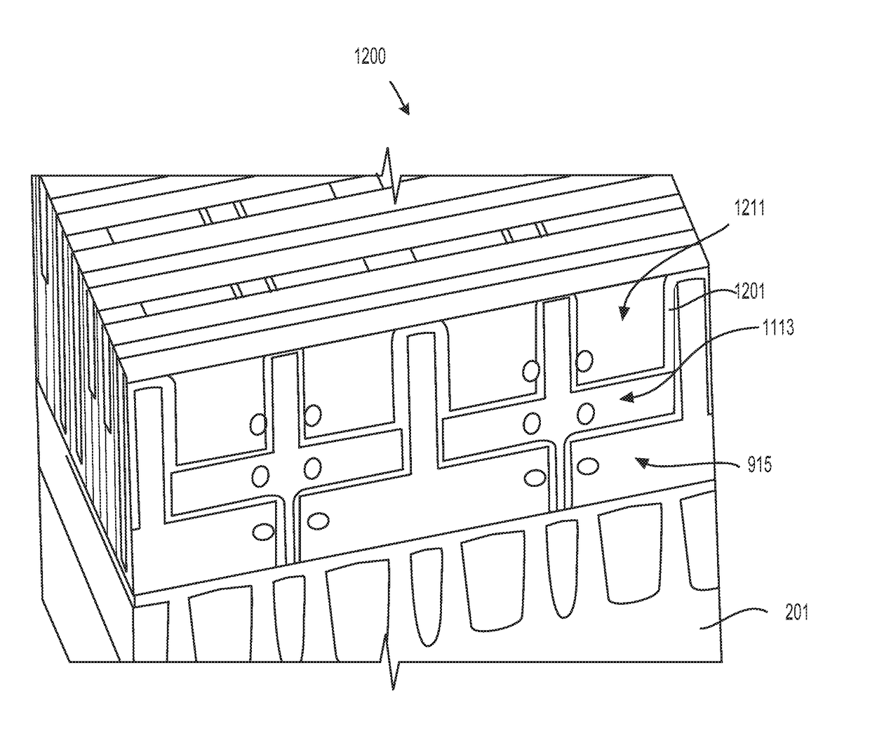
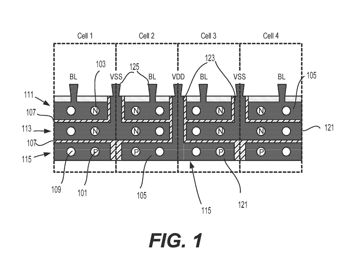
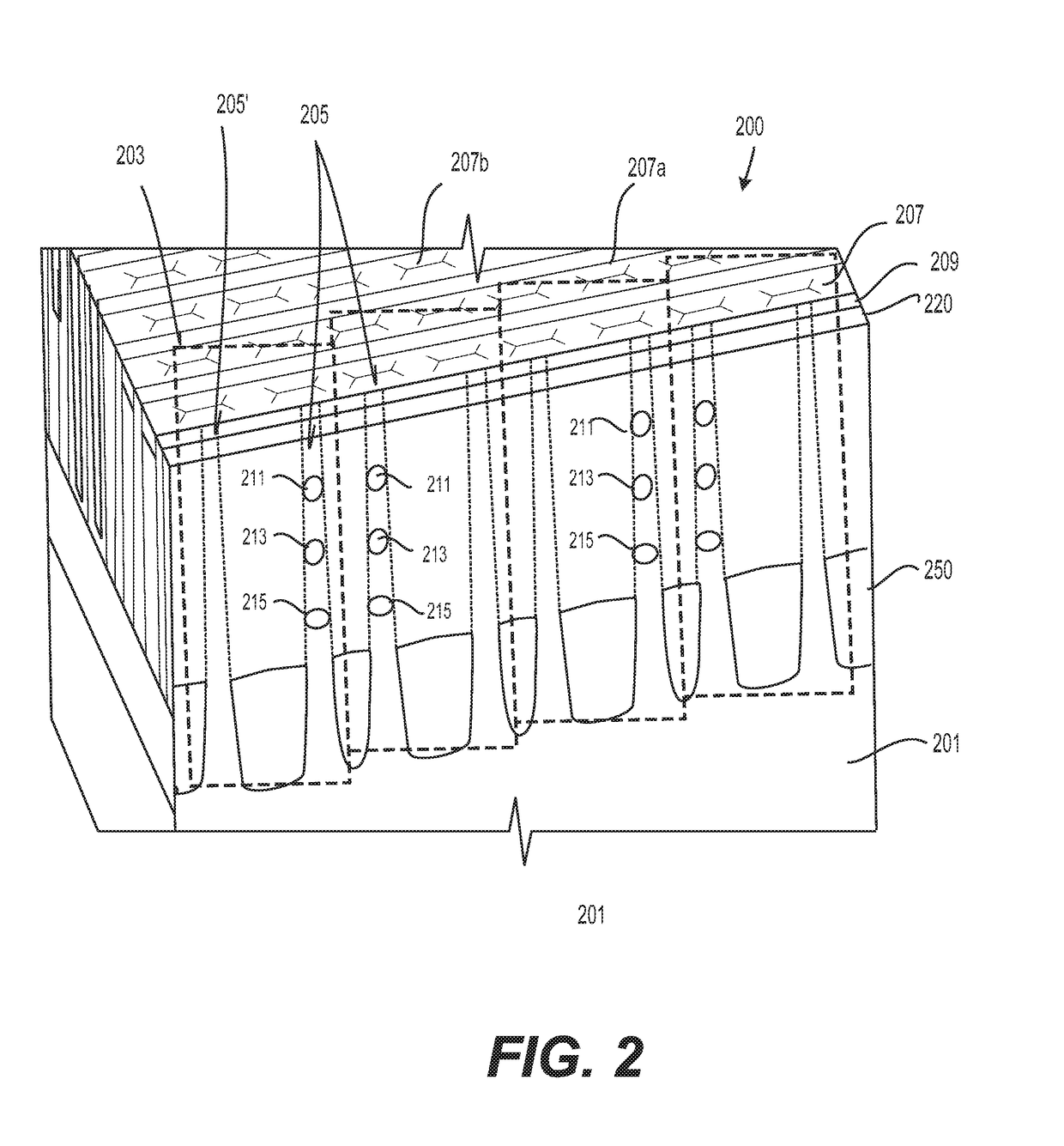
[0028]Techniques herein pertain to fabrication of 3D integrated circuits in which circuit devices are vertically arranged in relation to a planar surface of a substrate. According to disclosed embodiments, vertically arranged circuit devices can have electrodes formed in substantially the same plane with the respective device such that electrodes of the vertically arranged devices can be stacked or overlapped to occupy the same planar area. This can significantly improve area scaling capabilities for the integrated circuit. Techniques disclosed herein apply to stacking of active circuit devices (such as transistors), passive circuit devices (such as resistors, capacitors, inductors, etc.) or a combination of such devices into a 3D integrated circuit. Transistors may be field effect transistors (FET) devices using fin and / or multigate configurations, for example.

[0029]Aspects of this disclosure pertain to device fabrication using gate-all-around processing incorporating nanowires or ...


PUM


Abstract

A 3-D IC includes a substrate having a substrate surface. A first semiconductor device has a first electrical contact and is formed in a first area of the surface on a first plane substantially parallel to the substrate surface. A second semiconductor device has a second electrical contact and is formed in a second area of the surface on a second plane substantially parallel to the surface and vertically spaced from the first plane in a direction substantially perpendicular to the surface. A first electrode structure includes opposing top and bottom surfaces substantially parallel to the substrate surface, and a sidewall connecting the top and bottom surfaces such that the electrode structure forms a three dimensional electrode space. A conductive fill material is provided in the electrode space, and a dielectric layer electrically separates the conductive fill material into a first electrode electrically connected to the first contact of the first semiconductor device and a second electrode electrically connected to the second semiconductor device and electrically insulated from the first electrode. A first circuit terminal extends vertically from the top or bottom surface of the electrode structure and is electrically connected to the first electrode.

Description

CROSS REFERENCE TO RELATED APPLICATIONS[0001]This application is based on, and claims the benefit of priority to, U.S. provisional application No. 62 / 363,973 filed on Jul. 19, 2016, and to U.S. provisional application No. 62 / 372,106 filed Aug. 8, 2016, and to U.S. provisional application No. 62 / 373,164 filed on Aug. 10, 2016. The entire contents of each of these applications are incorporated herein by reference.BACKGROUNDField of the Disclosure[0002]The present invention relates to a semiconductor device and a method of manufacturing a semiconductor device such as an integrated circuit, and to manufacturing transistors and transistor components for an integrated circuit.Description of Related Art[0003]In the manufacture of a semiconductor device (especially on the microscopic scale), various fabrication processes are executed such as film-forming depositions, etch mask creation, patterning, material etching and removal, and doping treatments. These processes are performed repeatedly...

Claims


Application Information

Patent Timeline
IPC IPC(8): H01L27/11
CPCH01L27/1104H01L27/0688H01L21/823807H01L27/092H01L21/823871H01L21/823814H01L21/743H01L21/76897H01L21/76883H01L21/76834H10B10/125H10B10/00H10B10/12H01L21/823821H01L29/42392
Inventor SMITH, JEFFREYDEVILLIERS, ANTON
Owner TOKYO ELECTRON LTD
Learn More