Light emitting diode and method of fabricating the same

a technology of light-emitting diodes and light-emitting diodes, which is applied in the field of diodes, can solve the problems that the conventional light-emitting diodes with perovskite structures cannot achieve a satisfying requirement, and achieve the effect of improving luminous intensity and luminous efficiency of light-emitting diodes

Active Publication Date: 2018-02-01
NAT CHENG KUNG UNIV
View PDF0 Cites 6 Cited by
  • Summary
  • Abstract
  • Description
  • Claims
  • Application Information

AI Technical Summary

Benefits of technology

[0005]An object of the present disclosure is to provide a light emitting diode, which uses an active layer with a mesophase structure (also referred to as an intermediate structure) to improve a luminous intensity and a luminous efficiency of the light emitting diode.

Problems solved by technology

In general, the conventional light emitting diode with the perovskite structure cannot achieve a satisfying requirement on a highest luminous intensity and a luminous efficiency.

Method used


Image

  • Light emitting diode and method of fabricating the same
  • Light emitting diode and method of fabricating the same
  • Light emitting diode and method of fabricating the same

Examples


Embodiment Construction

[0021]The structure and the technical means adopted by the present disclosure to achieve the above and other objects can be best understood by referring to the following detailed description of the preferred embodiments and the accompanying drawings. Furthermore, directional terms described by the present disclosure, such as upper, lower, front, back, left, right, inner, outer, side, longitudinal / vertical, transverse / horizontal, etc., are only directions by referring to the accompanying drawings, and thus the used directional terms are used to describe and understand the present disclosure, but the present disclosure is not limited thereto.

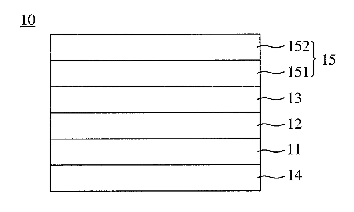
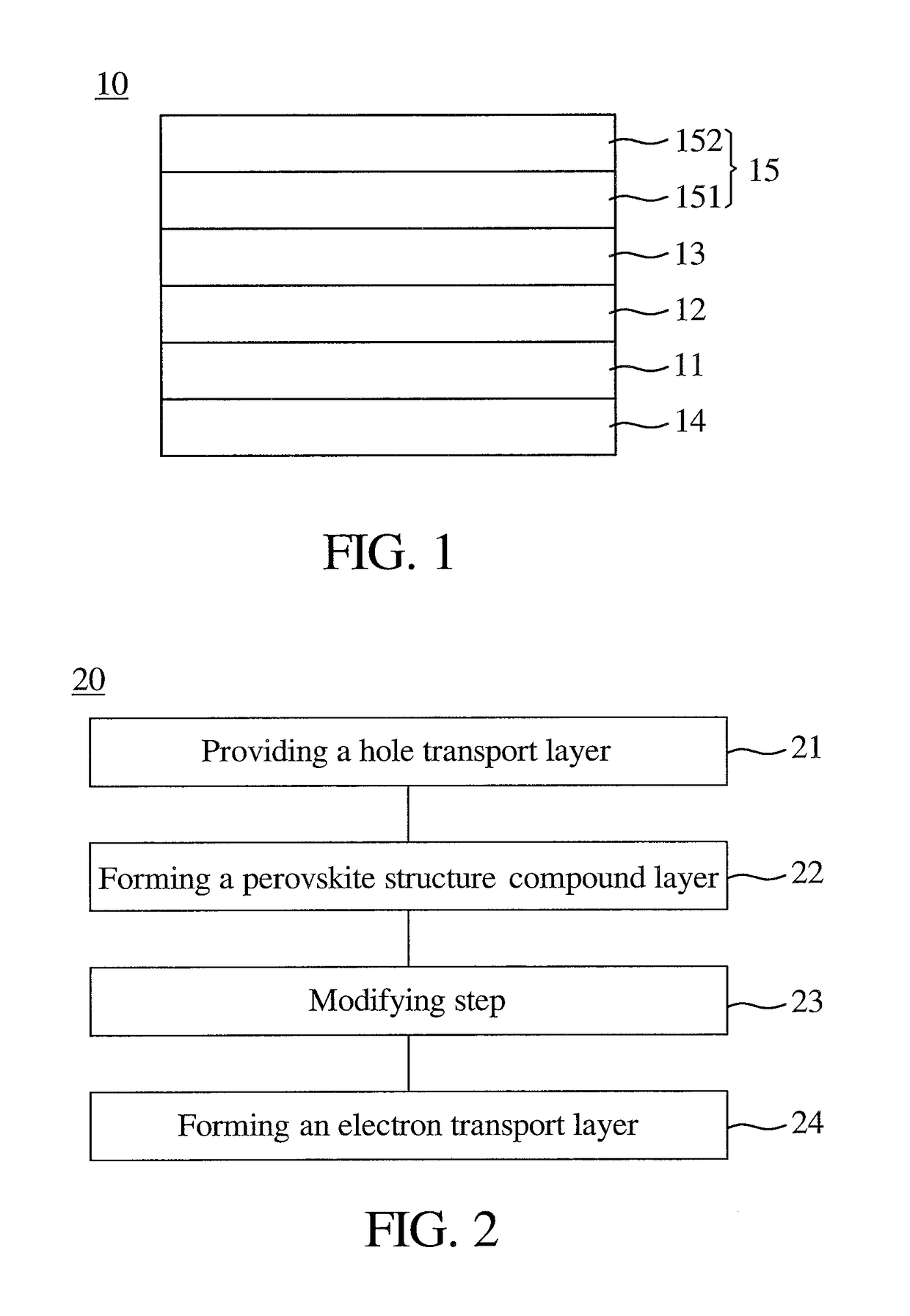
[0022]Please refer to FIG. 1, which is a cross-sectional schematic diagram of a light emitting diode 10 according to one embodiment of the present disclosure. In one embodiment of the present disclosure, the light emitting diode 10 includes a hole transport layer 11, an active layer 12, and an electron transport layer 13. In one embodiment, the ho...


PUM

PropertyMeasurementUnit
thicknessaaaaaaaaaa
thicknessaaaaaaaaaa
thicknessaaaaaaaaaa

Abstract

A light emitting diode and a method of fabricating the same are described. The light emitting diode has: a hole transport layer, an active layer and an electron transport layer. The active layer is disposed on the hole transport layer, and the active layer has a mesophase structure of an organic amine compound and a perovskite structure compound. The electron transport layer is disposed on the active layer.

Description

CROSS REFERENCE TO RELATED APPLICATION[0001]This application claims priority to U.S. Provisional Application No. 62 / 369,331, filed Aug. 1, 2016, titled “NiOx electrode interlayer and CH3NH2 / CH3NH3PbBr3 interface treatment to markedly advance hybrid perovskite-based light-emitting diodes”, which is incorporated herein by reference in its entirety.FIELD OF THE DISCLOSURE[0002]The present disclosure relates to a diode and a method of fabricating the same, and more particularly to a light emitting diode and a method of fabricating the same.BACKGROUND OF THE DISCLOSURE[0003]Currently, dye-sensitized solar cells (DSSC) have been developed to use an organic-inorganic hybrid perovskite crystalline material, methylammonium lead iodide (CH3NH3Pbl3), as a dye-sensitized light-absorbing layer, and organic polymers including (Poly (3,4-ethylenedioxythiophene): poly(styrene-sulfonate) (PEDOT: PSS) as a hole transport layer to prepare a solid state DSSC. However, a perovskite structure can also be...

Claims


Application Information

Patent Timeline
Patent Type & Authority Applications(United States)
IPC IPC(8): H01L51/00
CPCH01L51/0077H01L51/0008H01L51/0003H01L51/0029H01L2251/303H01L51/0035H01L51/5072H01L51/5012H01L51/5056H01L51/0037H10K85/00H10K50/00H10K50/15H10K50/16H10K71/00H10K50/115H10K85/50H10K85/30H10K71/12H10K71/16H10K71/811H10K85/111H10K85/1135H10K50/11H10K2102/00
Inventor GUO, TZUNG-FANG
Owner NAT CHENG KUNG UNIV
Why Eureka
Try Eureka