Light emitting device and electronic device

a technology of light emitting devices and electronic devices, which is applied in the direction of discharge tubes/lamp details, discharge tubes luminescnet screens, natural mineral layered products, etc., can solve the problems of small voltage and luminance efficiency reduction, low productivity, and low number of processes, so as to reduce voltage and luminance efficiency, improve color purity, and reduce power consumption

Inactive Publication Date: 2007-01-04
SEMICON ENERGY LAB CO LTD
View PDF50 Cites 93 Cited by
  • Summary
  • Abstract
  • Description
  • Claims
  • Application Information

AI Technical Summary

Benefits of technology

[0011] It is another object of the present invention to provide a light emitting element and a light emitting device which can achieve both low power consumption and the improvement of color purity without appearance of an adverse effect such as reduction in voltage and luminance efficiency.
[0013] Another feature of the present invention is that a thickness of the buffer layer of the light emitting element is determined so that intensity of light emitted to outside the light emitting element becomes high. An emission spectrum of a light emitting layer or a light emitting substance and an emission spectrum of a light emitting element may be compared with each other in order to examine whether emission intensity of the light emitting element is heightened. When a half value width of an emission spectrum of the former is narrower than that of the latter, emission intensity is heightened. More specifically, when the half value width of an emission spectrum of the former is in the range of 80% or less, and 30% or more and 80% or less of the half value width of the latter, it can be considered that emission intensity of the light emitting element is heightened.
[0021] According to the light emitting element and the light emitting device of the present invention, low power consumption and the improvement of color purity can be easily achieved at the same time without appearance of an adverse effect such as reduction in voltage and luminance efficiency.

Problems solved by technology

In addition, a requirement of reducing energy consumption is more and more increased in association with an environmental problem, an energy problem, and the like in a television, a display, and the like in addition to a mobile device.
In addition, in the structure in Patent Document 2, the reduction in voltage and luminance efficiency is small.
However, in order to form a transparent electrode corresponding to each color, the number of processes is increased because one of the electrodes of the light emitting element is formed so as to form a transparent electrode corresponding to each color, and productivity is very low.

Method used


Image

  • Light emitting device and electronic device
  • Light emitting device and electronic device
  • Light emitting device and electronic device

Examples


embodiment mode 1

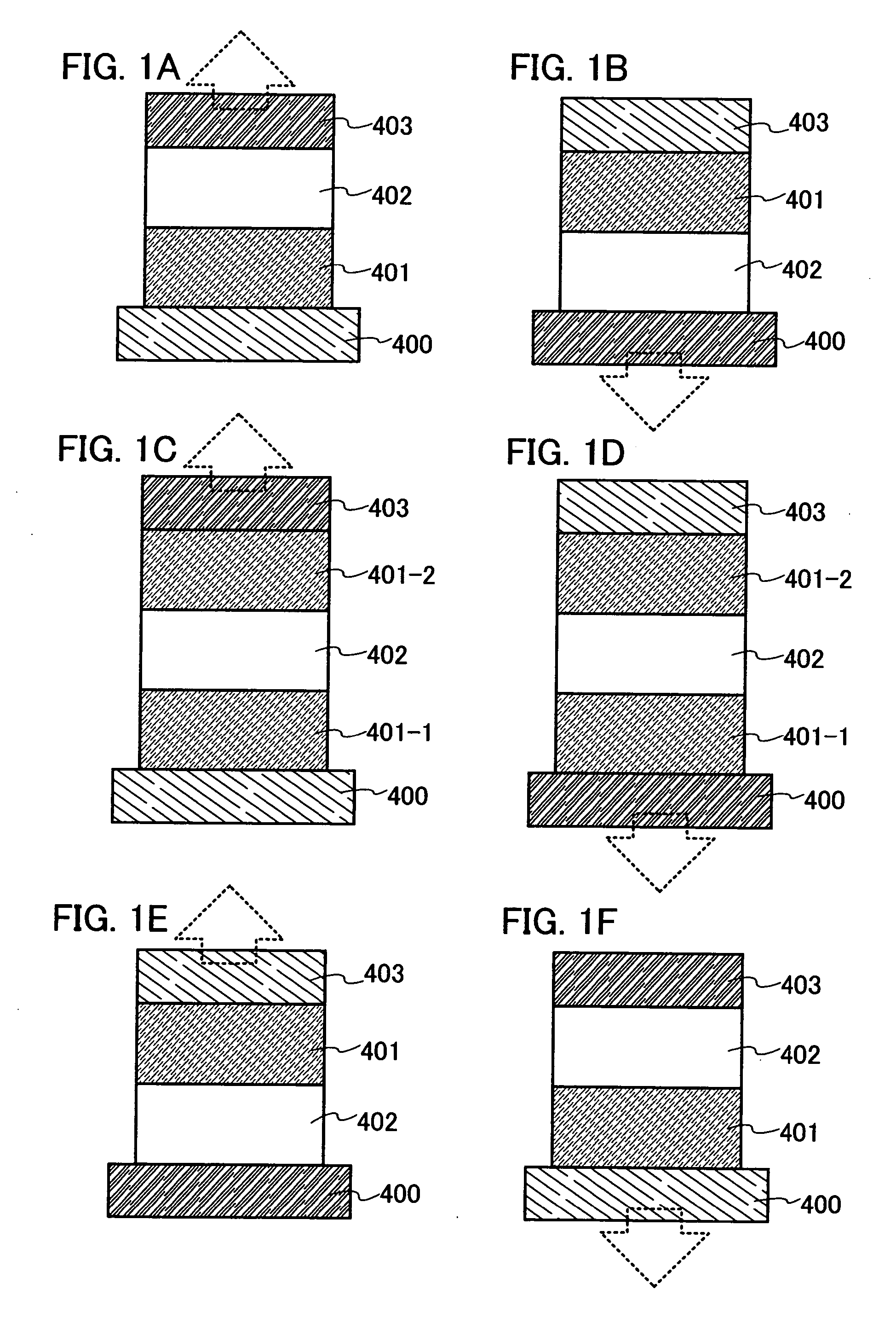
[0037]FIG. 1A is a frame format showing one mode of a light emitting element of the present invention. In a light emitting element of the present invention in FIG. 1A, a layer including an organic compound formed by a buffer layer 401 and a light emitting laminated body 402 is sandwiched between a pair of electrodes composed of a first electrode 400 and a second electrode 403 over an insulator which is not shown. In FIG. 1A, a structure in which light is extracted from a second electrode 403 side will be explained.

[0038] Although the first electrode 400 may be formed to have a single layer or a multilayer, the first electrode 400 is formed to be an electrode having high reflectance. Although the second electrode 403 may be formed to have a single layer or a multilayer, the second electrode 403 is formed as a translucent electrode with respect to light emitted from the light emitting element. According to the light emitting element of the present invention, light emission can be obt...

embodiment mode 2

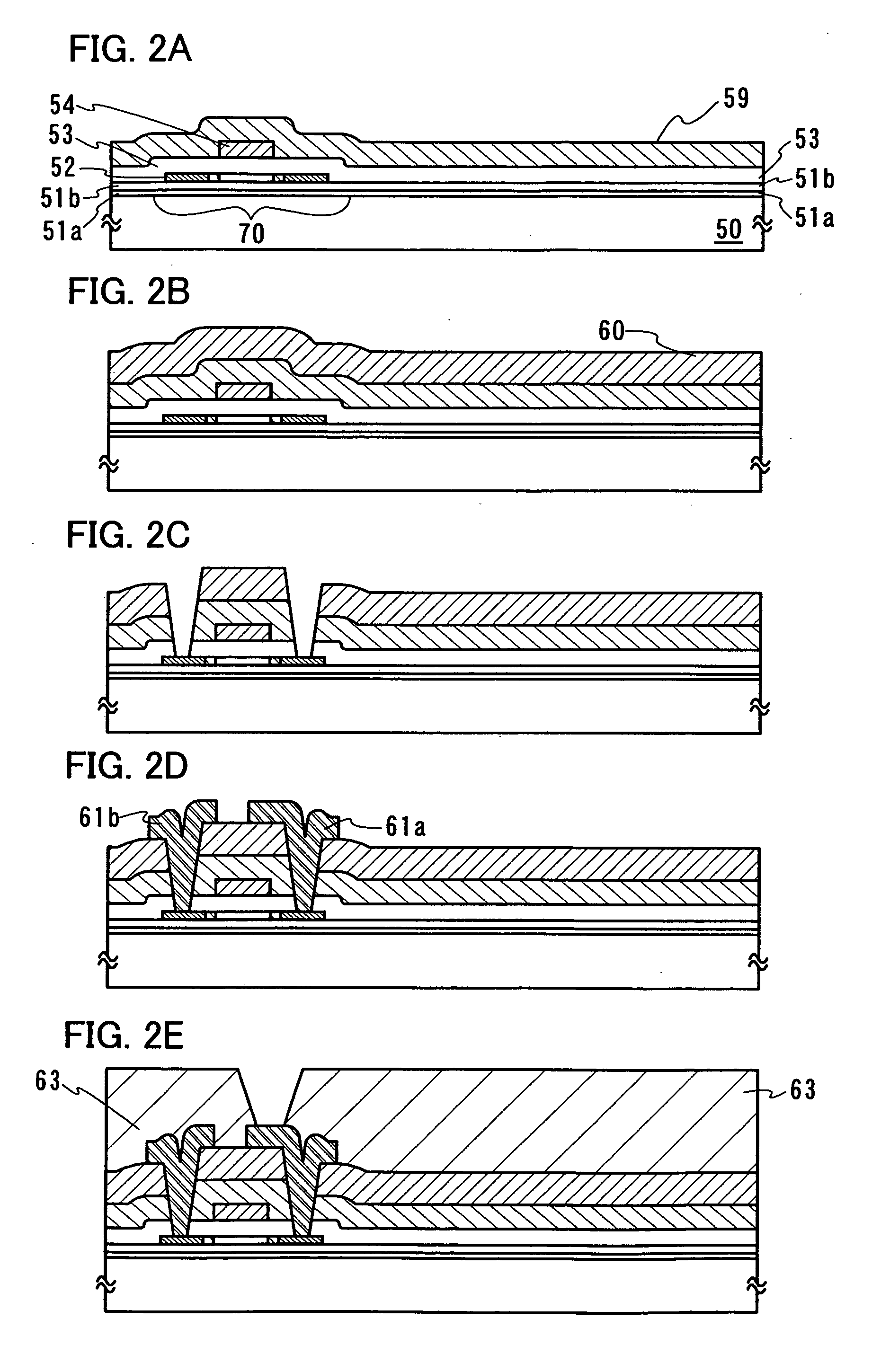
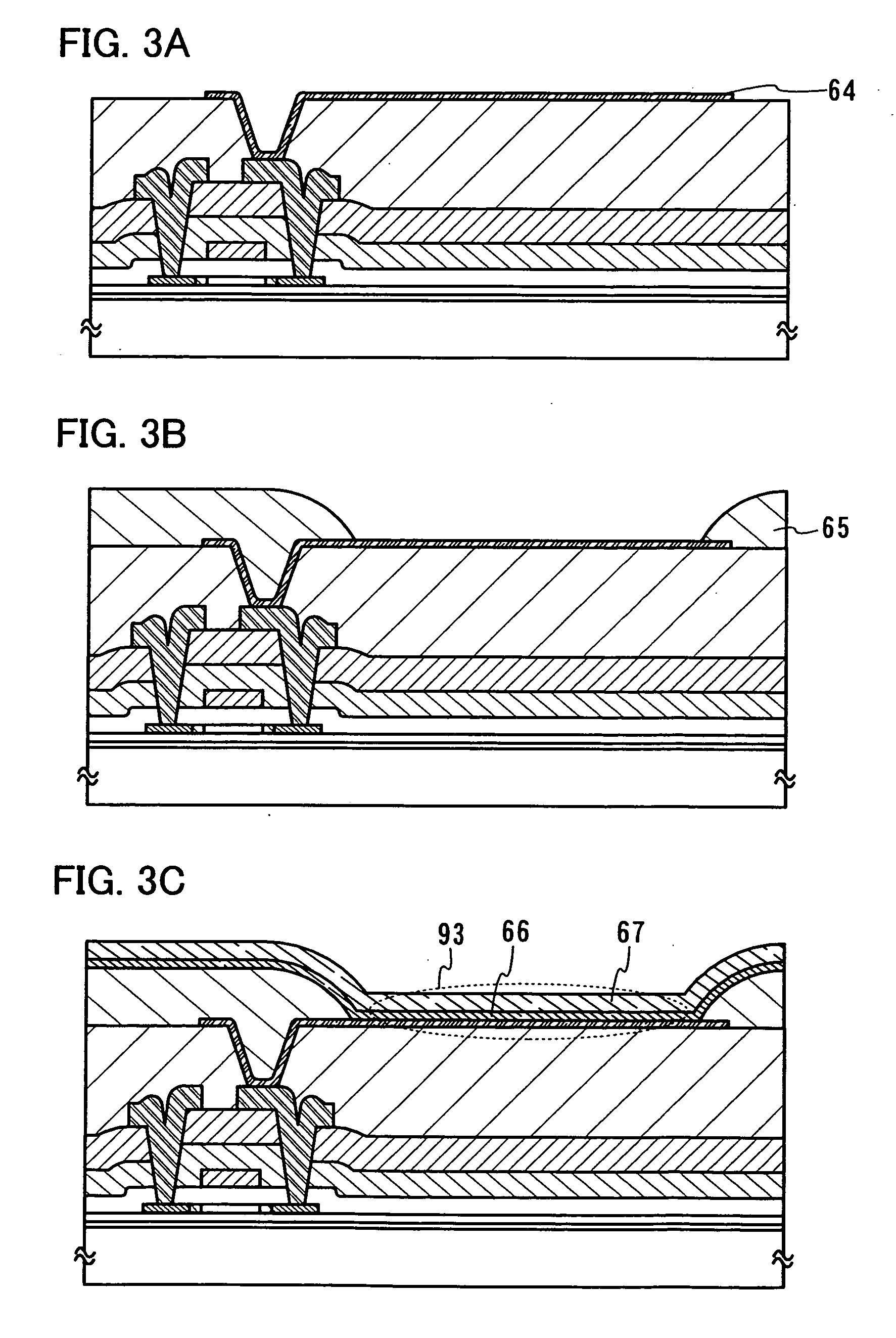
[0163] In this embodiment mode, a manufacturing method of a light emitting device of the present invention will be explained with reference to FIGS. 2A to 2E, FIGS. 3A to 3C, and FIG. 4. It is to be noted that an example of manufacturing an active matrix light emitting device in which light is emitted to a second electrode side is shown in this embodiment mode. In a case of full color display using light emitting elements each having a different wavelength, the arrangement of a pixel of each color is not particularly limited, and desired arrangement such as stripe arrangement or delta arrangement can be applied. In particular, the delta arrangement in which each of the pixels are arranged in a delta array can be preferably applied in a case of using a light emitting element exhibiting three types of luminescent color such as red, green, and blue. The pixel of the delta arrangement is ideal for a light emitting device which displays an image such as a television.

[0164] As a matter o...

embodiment mode 3

[0202] In this embodiment mode, an outer appearance of a panel of an active matrix light emitting device, which is a display device of the present invention, will be described with reference to FIGS. 5A and 5B. FIG. 5A is a top view of a panel in which a transistor and a light emitting element formed over a substrate are sealed with a sealing material that is formed between the substrate and a counter substrate 4006. FIG. 5B is a cross-sectional view of FIG. 5A. The light emitting element of this panel has a structure as shown in Embodiment Mode 1.

[0203] A sealing material 4005 is provided so as to surround a pixel portion 4002, a signal line driver circuit 4003, and a scanning line driver circuit 4004 that are provided over a substrate 4001. The counter substrate 4006 is provided over the pixel portion 4002, the signal line driver circuit 4003, and the scanning line driver circuit 4004. Thus, the pixel portion 4002, the signal line driver circuit 4003, and the scanning line driver...


PUM

PropertyMeasurementUnit
reflectanceaaaaaaaaaa
thicknessaaaaaaaaaa
thicknessaaaaaaaaaa

Abstract

Color purity of a light emitting element is improved without an adverse effect such as reduction in voltage and luminance efficiency. The light emitting element has a light emitting laminated body including a light emitting layer between a pair of electrodes. A buffer layer is provided to be in contact with at least one of the electrodes. One of the electrodes is an electrode having high reflectance and the other is a translucent electrode. By employing a translucent electrode, light can be transmitted and reflected. An optical distance between the electrodes is adjusted in accordance with a thickness of the buffer layer, and accordingly, light can be resonated between the electrodes. The buffer layer is made of a composite material including an organic compound and a metal compound; therefore, voltage and luminance efficiency of the light emitting element is not affected even if a distance between the electrodes becomes long.

Description

BACKGROUND OF THE INVENTION [0001] 1. Field of the Invention [0002] The present invention relates to a light emitting element which emits light by feeding current and a light emitting device using the light emitting element. [0003] 2. Description of the Related Art [0004] A light emitting device using a light emitting element having a layer including an organic material between a pair of electrodes which emits light by feeding current between the electrodes has been developed. Such a light emitting device is advantageous to be a thin shape and lightweight compared with other display devices which are referred to as thin display devices, has favorable visibility because of self-light emission, and has high response speed. Therefore, the light emitting devices are actively developed as display devices for the next generation, and at the present day, part of the light emitting devices is in practical use. [0005] In such a light emitting element, holes are injected from an electrode whi...

Claims


Application Information

Patent Timeline
Patent Type & Authority Applications(United States)
IPC IPC(8): H01L51/52H05B33/12
CPCH01L51/5052H01L51/5092H01L27/326H01L51/5265H10K50/165H10K50/852H05B33/14H05B33/26H10K50/171H10K59/121
Inventor NOMURA, RYOJISEO, SATOSHIIWAKI, YUJISUGISAWA, NOZOMU
Owner SEMICON ENERGY LAB CO LTD
Why Eureka
Try Eureka