Wire to board connectors suitable for use in bypass routing assemblies

a technology of wire-to-board connectors and bypass routing, which is applied in the direction of coupling devices, coupling contact members, two-part coupling devices, etc., can solve the problems of high-speed signal transmission line loss of fr4 material, increase the final cost of the device, and undesirable fr4 material. , to achieve the effect of low loss characteristics

Active Publication Date: 2018-02-01
MOLEX INC
View PDF23 Cites 73 Cited by
  • Summary
  • Abstract
  • Description
  • Claims
  • Application Information

AI Technical Summary

Benefits of technology

[0009]Accordingly, there are provided herein, improved high speed bypass assemblies which utilize cables, rather than circuit boards, to define signal transmission lines which are useful for high speed data applications at 10 Gbps and above and with low loss characteristics.

Problems solved by technology

Although inexpensive, FR4 is known to be lossy in high speed signal transmission lines which transfer data at rates of about 6 Gbps and greater.
These losses increase as the speed increases and therefore make FR4 material undesirable for the high speed data transfer applications of about 10 Gbps and greater.
In order to use FR4 as a circuit board material for signal transmission lines, a designer may have to utilize amplifiers and equalizers, which increase the final cost of the device.
The overall length of the signal transmission lines in FR4 circuit boards can exceed threshold lengths, about 10 inches, and may include bends and turns that can create signal reflection and noise problems as well as additional losses.
Losses can sometimes be corrected by the use of amplifiers, repeaters and equalizers but these elements also increase the cost of manufacturing the final circuit board.
This complicates the layout of the circuit board as additional board space is needed to accommodate these amplifiers and repeaters.
These turns and the transitions which occur at termination points along the signal transmission lines may negatively affect the integrity of the signals transmitted thereby.
It then becomes difficult to route transmission line traces in a manner to achieve a consistent impedance and a low signal loss therethrough.
Custom materials, such as MEGTRON, are available for circuit board construction which reduces such losses, but the prices of these materials severely increases the cost of the circuit board and, consequently, the electronic devices in which they are used.
FR4 circuit board materials can handle data transmission speeds of 10 Gbits / sec, but this handling comes with disadvantages.
Therefore, designers find it difficult to provide “green” designs for such devices, as low power chips cannot effectively drive signals for such and longer lengths.
The higher power needed to drive the signals consumes more electricity and it also generates more heat that must be dissipated.
Accordingly, these disadvantages further complicate the use of FR4 as a motherboard material used in electronic devices.
Using more expensive, and exotic motherboard materials, such as MEGTRON, to handle the high speed signals at more acceptable losses increases the overall cost of electronic devices.
Notwithstanding the low losses experienced with these expensive materials, they still require increased power to transmit their signals and incurred, and the turns and crossovers required in the design of lengthy board traces create areas of signal reflection and potential increased noise.
It therefore becomes difficult to adequately design signal transmission lines in circuit boards and backplanes to meet the crosstalk and loss requirements needed for high speed applications.
Although it is desirable to use economical board materials such as FR4, the performance of FR4 falls off dramatically as the data transmission rate approaches 10 Gbps, driving designers to use more expensive board materials and increasing the overall cost of the device in which the circuit board is used.

Method used


Image

  • Wire to board connectors suitable for use in bypass routing assemblies
  • Wire to board connectors suitable for use in bypass routing assemblies
  • Wire to board connectors suitable for use in bypass routing assemblies

Examples


Embodiment Construction

[0057]While the Present Disclosure may be susceptible to embodiment in different forms, there is shown in the Figures, and will be described herein in detail, specific embodiments, with the understanding that the Present Disclosure is to be considered an exemplification of the principles of the Present Disclosure, and is not intended to limit the Present Disclosure to that as illustrated.

[0058]As such, references to a feature or aspect are intended to describe a feature or aspect of an example of the Present Disclosure, not to imply that every embodiment thereof must have the described feature or aspect. Furthermore, it should be noted that the description illustrates a number of features. While certain features have been combined together to illustrate potential system designs, those features may also be used in other combinations not expressly disclosed. Thus, the depicted combinations are not intended to be limiting, unless otherwise noted.

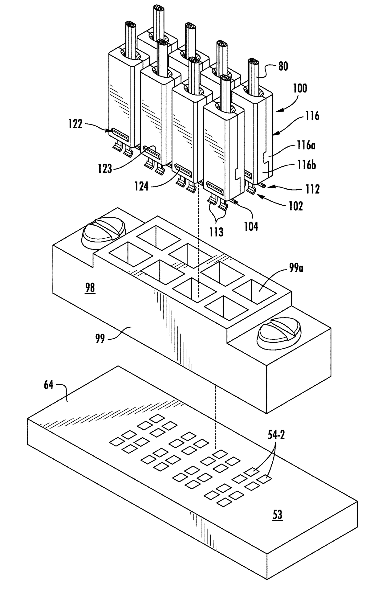
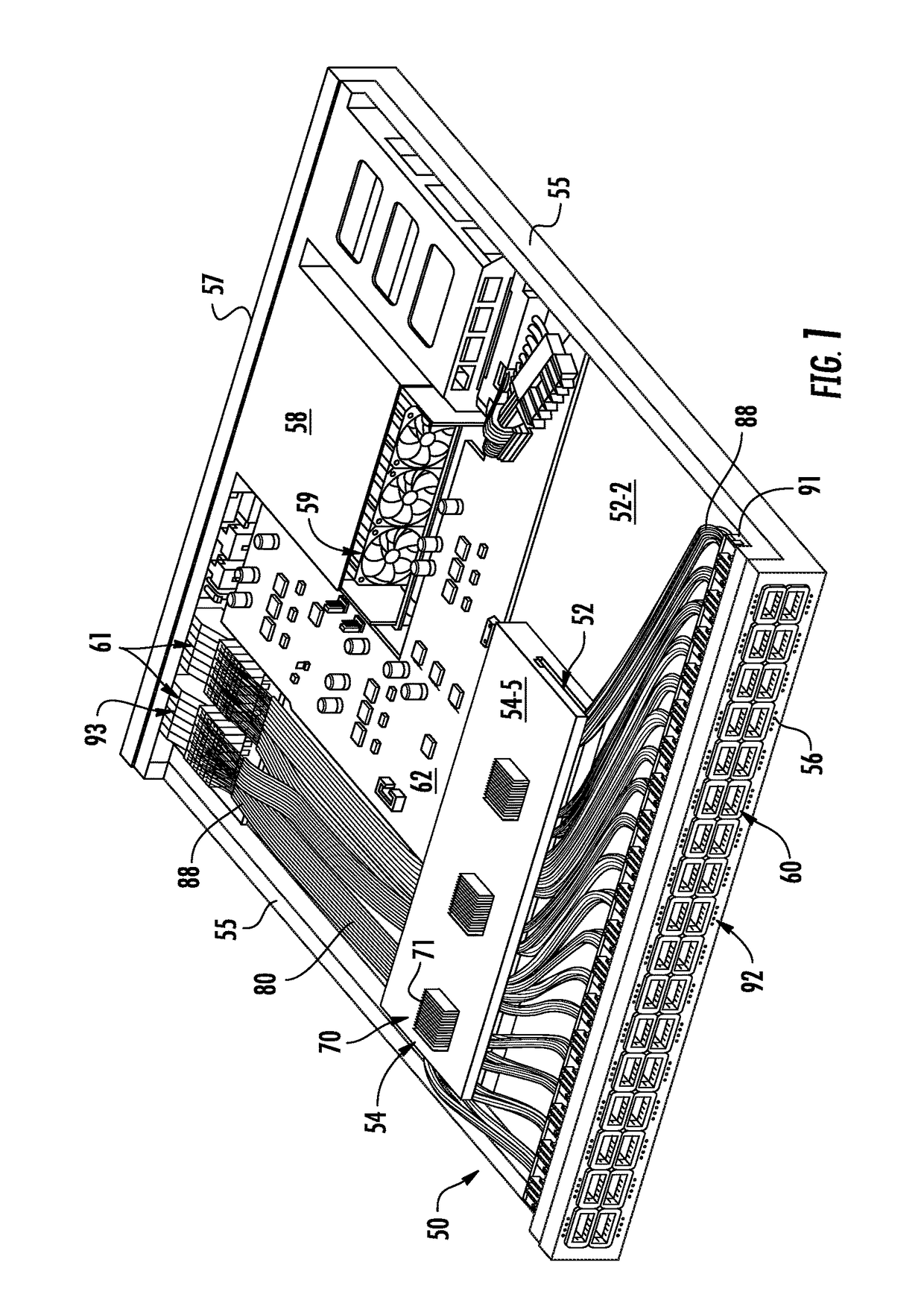
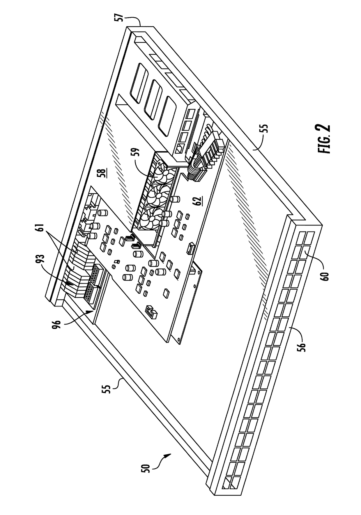
[0059]In the embodiments illustrated in ...


PUM


Abstract

A wire to board connector is provided for connecting cables of cable bypass assemblies to circuitry mounted on a circuit board. The connector has a structure that maintains the geometry of the cable through the connector. The connector includes a pair of edge coupled conductive signal terminals and a ground shield to which the signal terminals are broadside coupled. The connector includes a pair of ground terminals aligned with the signal terminals and both sets of terminals have J-shaped contact portions that flex linearly when the connector is inserted into a receptacle. In another embodiment, the signal terminal contact portions are supported by a compliant member that may deflect when the connectors engage contact pads on a substrate.

Description

REFERENCE TO RELATED APPLICATIONS[0001]This application claims priority of prior U.S. provisional patent application No. 62 / 102,045, filed Jan. 11, 2015 entitled “The Molex Channel”; prior U.S. provisional patent application No. 62 / 102,046, filed. Jan. 11, 2015 entitled “The Molex Channel”; prior U.S. provisional patent application No. 62 / 102,047, filed Jan. 11, 2015 entitled “The Molex Channel”; prior U.S. provisional patent application No. 62 / 102,048 filed Jan. 11, 2015 entitled “High Speed Data Transmission Channel Between Chip And External Interfaces Bypassing Circuit Boards”; prior U.S. provisional patent application No. 62 / 156,602, filed May 4, 2015, entitled “Free-Standing Module Port And Bypass Assemblies Using Same”, prior U.S. provisional patent application No. 62 / 156,708, filed May 4, 2015, entitled “Improved Cable-Direct Connector”; prior U.S. provisional patent application No. “62 / 167,036, filed May 27, 2015 entitled “Wire to Board Connector with Wiping Feature and Bypa...

Claims


Application Information

Patent Timeline
Patent Type & Authority Applications(United States)
IPC IPC(8): H01R12/71H01R13/627H01R12/75H01R13/11H01R24/22H01R24/60
CPCH01R12/714H01R12/71H01R24/22H01R24/60H01R12/716H01R12/75H01R13/113H01R13/6275H01R13/639H01R13/567
Inventor LLOYD, BRIAN KEITHWALZ, GREGORY B.REED, BRUCEFITZGERALD, GREGORYISAAC, AYMANREGNIER, KENT E.JANOWIAK, BRANDONSCHULZ, DARIAN R.AHMAD, MUNAWARJONES, ERAN J.RESENDEZ, JAVIERROST, MICHAEL
Owner MOLEX INC
Why Eureka
Try Eureka