

Conductive structure and electronic device comprising same
a technology of conductive structure and electronic device, which is applied in the direction of conductive layers on insulating supports, inorganic insulators, conductors, etc., can solve the problems of lowering device efficiency, and achieve low surface resistance value, low light transmittance change, and high light transmittance
- Summary
- Abstract
- Description
- Claims
- Application Information
AI Technical Summary
Benefits of technology
Problems solved by technology
Method used
Image

Examples
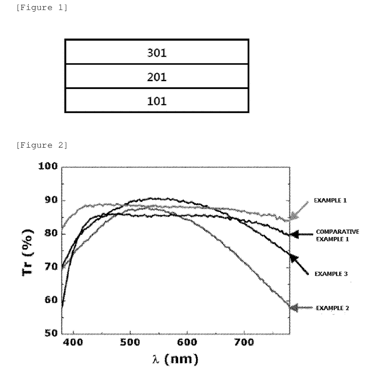
example 1
[0073]A first dielectric layer was formed by depositing Hf oxide on a glass substrate by using an RF sputter method. A metal layer made of Ag was deposited to a thickness of 10 nm on the first dielectric layer by using a DC sputter method and Nb oxide was deposited on the metal layer as a second dielectric layer to manufacture a conductive structure body.
example 2
[0074]A first dielectric layer was formed by depositing Hf oxide on a glass substrate by using an RF sputter method. A metal layer made of Ag was deposited to a thickness of 18 nm on the first dielectric layer by using a DC sputter method and Hf oxide was deposited on the metal layer as a second dielectric layer to manufacture a conductive structure body.
example 3
[0075]A first dielectric layer was formed by depositing Hf oxide on a glass substrate by using an RF sputter method. A metal layer made of Ag was deposited to a thickness of 13 nm on the first dielectric layer by using a DC sputter method and Nb oxide was deposited on the metal layer as a second dielectric layer to manufacture a conductive structure body.
PUM
| Property | Measurement | Unit |
|---|---|---|
| mean refractive index | aaaaa | aaaaa |
| total thickness | aaaaa | aaaaa |
| thickness | aaaaa | aaaaa |
Abstract
Description
Claims
Application Information