
Polishing head, cmp apparatus including a polishing head, and manufacturing method of semiconductor integrated circuit device using a cmp apparatus

Active Publication Date: 2018-02-15
ABLIC INC
View PDF0 Cites 0 Cited by
  • Summary
  • Abstract
  • Description
  • Claims
  • Application Information

AI Technical Summary

Benefits of technology

The technical effects of this patent are to create a polishing head that can transmit uniform pressure to a wafer during a chemical mechanical polishing (CMP) process, resulting in reduced thickness fluctuations of the wafer's polishing target material throughout the entire wafer plane. This is achieved by using an air bag, a stress distributing plate, and shock absorbing sheets to achieving uniformity in pressure distribution. Additionally, the CMP apparatus and semiconductor integrated circuit device manufacturing method that uses this apparatus are also reduced in thickness fluctuations.

Problems solved by technology

Fluctuation in electrical characteristics takes place in wafer regions where the fluctuation of the film thickness took place, which may cause anomaly in electrical characteristics.
The head structure consequently makes the CMP apparatus large in scale and requires a complicate control mechanism.

Method used


Image

  • Polishing head, cmp apparatus including a polishing head, and manufacturing method of semiconductor integrated circuit device using a cmp apparatus
  • Polishing head, cmp apparatus including a polishing head, and manufacturing method of semiconductor integrated circuit device using a cmp apparatus
  • Polishing head, cmp apparatus including a polishing head, and manufacturing method of semiconductor integrated circuit device using a cmp apparatus

Examples


first embodiment

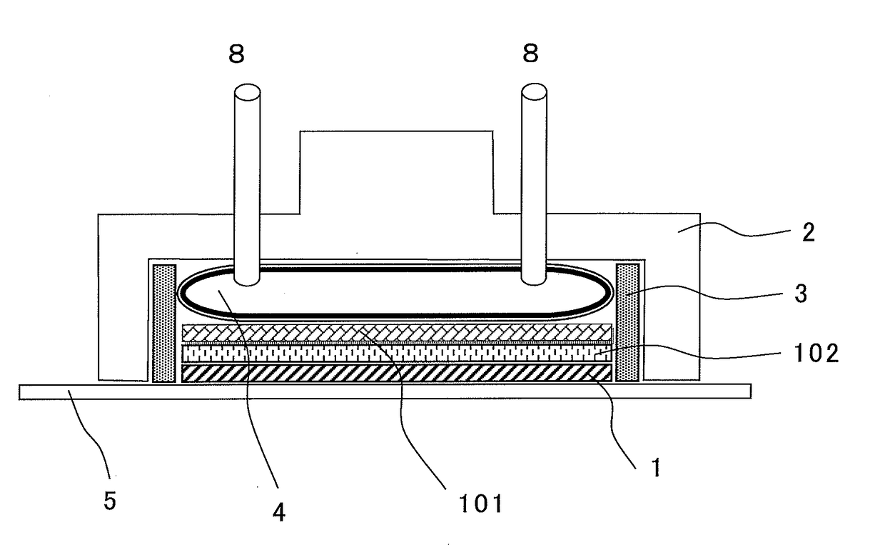
[0027]FIG. 1 is a schematic sectional view of the present invention for schematically illustrating, in particular, the sectional structure of a head portion of a CMP apparatus. As described above, in prior art illustrated in FIG. 9, when compressed air is introduced to the air bag, the high air pressure higher than the pressure in the central portion is applied locally to the region 6 in the peripheral portion of the air bag. In the portion of the wafer 1 that is pressed down from above by the high pressure portion 6, the rate of polishing a polishing target material (for example, insulating film) rises in the region, where the pressure is intense, and more polishing target material is polished off than in the central portion where the wafer 1 is pressed under less pressure. The in-plane uniformity of the polishing target material located in the region 6 in the wafer 1 after the planarizing is consequently poor.

[0028]In the CMP apparatus of FIG. 1, an air bag 4 is placed on a back s...

second embodiment

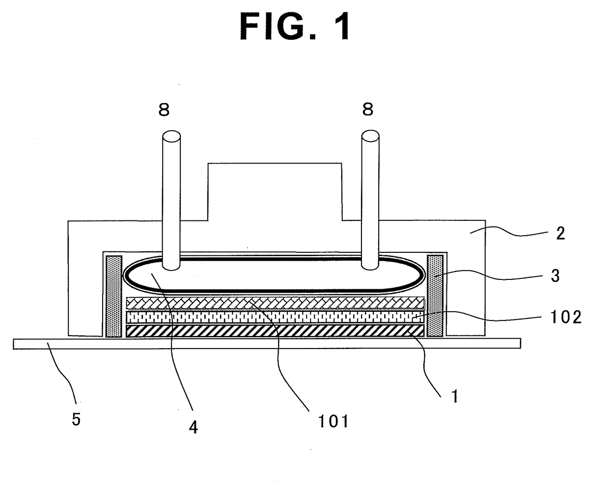
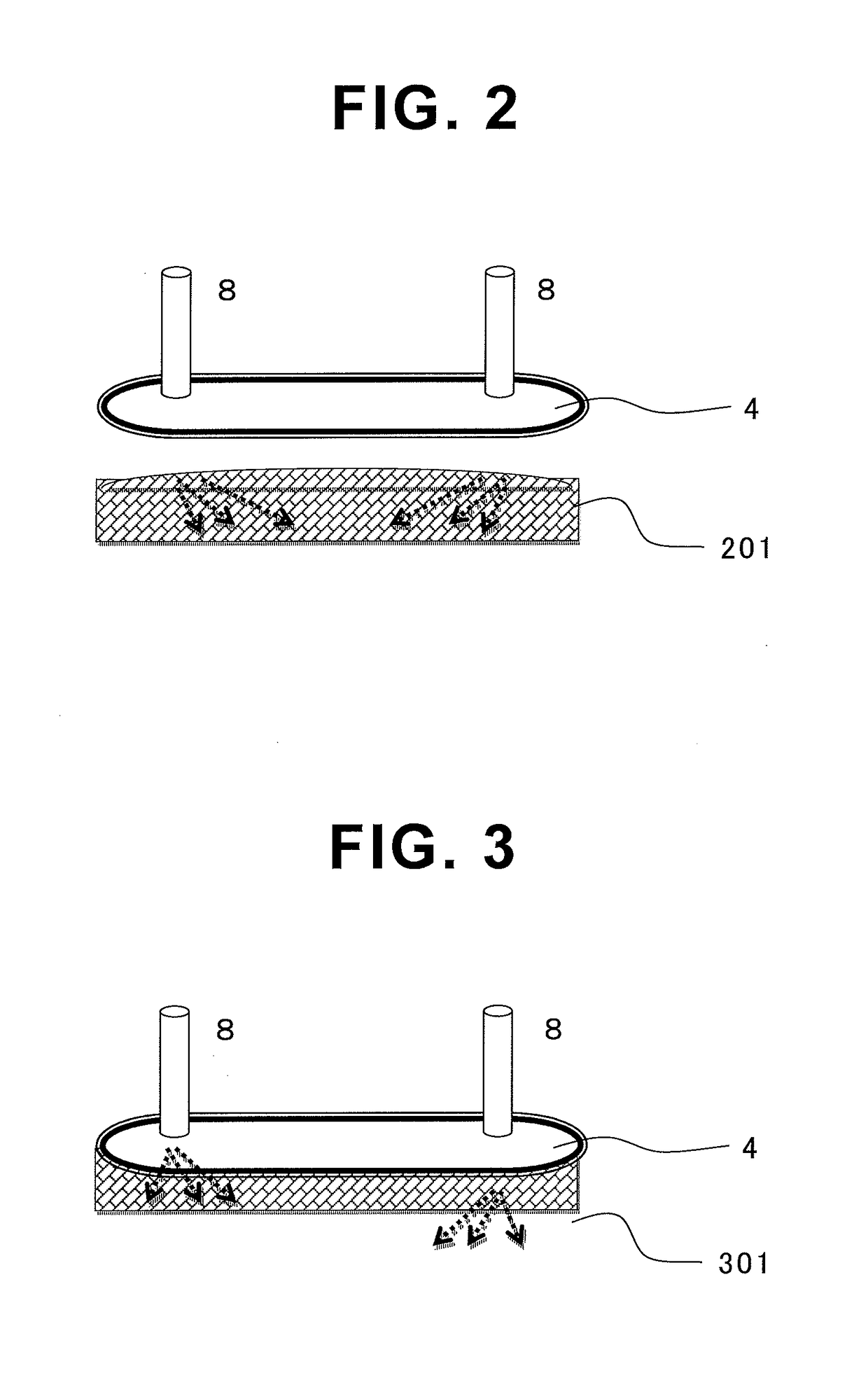
[0034]FIG. 2 is a schematic sectional view for illustrating the present invention. FIG. 2 is a simplified illustration of a CMP apparatus in which only the air bag 4 and a stress distributing plate 201 under the air bag 4 are illustrated, and a shock absorbing sheet and other components below the stress distributing plate 201 are omitted. First, a high pressure region 6 to which high air pressure is applied locally as illustrated in FIG. 9 is already known in prior art, which is a region where the increased rate of polishing the polishing target material lowers the uniformity of planarization. Locally high pressure applies to the region 6 because the pressure from the air bag 4 is high in a portion that is close to an air flow inlet / outlet and to the retainer ring 3.

[0035]While the stress distributing plate 101 of the first embodiment is structured so as to have a uniform thickness, the stress distributing plate 201 of the second embodiment illustrated in FIG. 2 is structured so as ...


PUM


Abstract

In a polishing head for a CMP apparatus, a stress distributing plate made of metal or ceramic is placed between a wafer on a polishing pad and an air bag configured to press down the wafer, and a shock absorbing sheet is provided between the stress distributing plate and the underlying wafer, to thereby make pressure applied from the air bag to the wafer uniform.

Description

BACKGROUND OF THE INVENTION1. Field of the Invention[0001]The present invention relates to a structure of a polishing head for a CMP apparatus configured to planarize a wafer plane uniformly throughout the wafer plane, a CMP apparatus including the polishing head, and a manufacturing method of a semiconductor integrated circuit device using the CMP apparatus.2. Description of the Related Art[0002]In recent years, new microfabrication technologies have been developed as the level of integration and performance of semiconductor integrated circuits (hereinafter referred to as LSIs) has increased. Chemical mechanical polishing (hereinafter also referred to as CMP with the initials of each word) is one of the new technologies, and is used frequently in LSI manufacturing processes, in particular, in the processes such as planarization of an interlayer insulating film, formation of a metal plug, and formation of embedded wiring of a multi-layer wiring forming process.[0003]The basic struct...

Claims


Application Information

Patent Timeline
IPC IPC(8): B24B37/04B24B37/005B24B49/00H01L21/304B24B49/10
CPCB24B37/042H01L21/304B24B37/005B24B49/006B24B49/10B24B37/11B24B37/34B24B55/00B24B37/30B24B37/32B24B41/047B24B37/04B24B57/02H01L21/30625
Inventor YAMAMOTO, SUKEHIRO
Owner ABLIC INC
Learn More