Liquid crystal display device

a liquid crystal display and display device technology, applied in non-linear optics, instruments, optics, etc., can solve the problems of easy to see display unevenness, light leakage, and display unevenness, and achieve the effect of enhancing the screen resolution of liquid crystal display devices, especially small ones, and reducing the distance between the through-hole in the pixel and the through-hole in the adjacent pixel

Active Publication Date: 2018-02-15
JAPAN DISPLAY INC
View PDF2 Cites 8 Cited by
  • Summary
  • Abstract
  • Description
  • Claims
  • Application Information

AI Technical Summary

Benefits of technology

[0006]The screen resolution of liquid crystal display devices, especially small ones, is being enhanced. Enhancing resolution requires the area of each pixel to be reduced. This means that within a pixel, the area of the through-hole used to connect the pixel electrode to the source electrode of the TFT occupies a larger portion of that pixel. Moreover, the distance between the through-hole in the pixel and the through-hole in an adjacent pixel is reduced as well.

Problems solved by technology

The areas where the alignment film is not formed will cause light leakage.
However, if multiple regions where the alignment film is not formed are connected to one another, the whole area where the alignment film is not formed becomes larger, resulting in display unevenness.
Regions where the alignment film is not formed are present in multiple pixels, and those regions are connected to one another, causing display unevenness that can be easily seen.

Method used


Image

  • Liquid crystal display device
  • Liquid crystal display device
  • Liquid crystal display device

Examples


embodiment 1

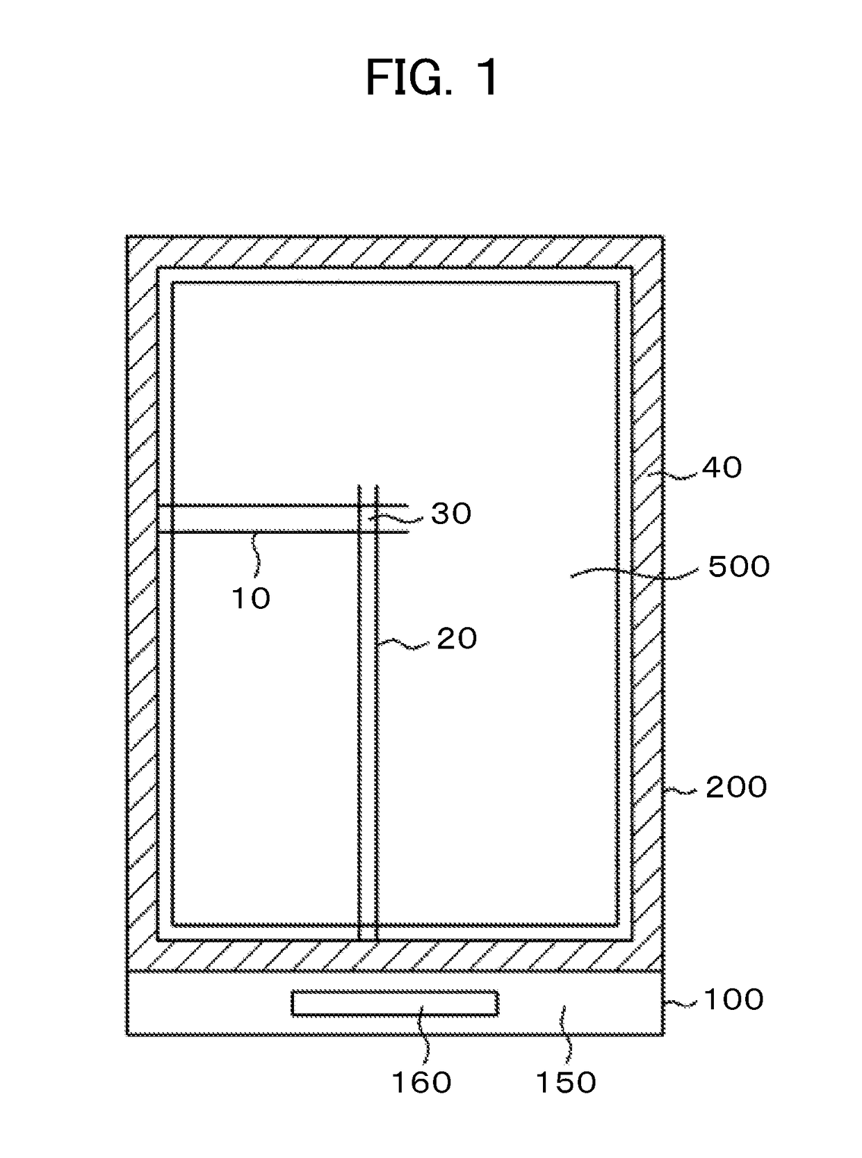
[0034]FIG. 1 is a plan view of a liquid crystal display device to which the invention is applied. In FIG. 1, a TFT substrate 100 and a counter substrate 200 are glued by a sealing material 40, and a liquid crystal layer is sandwiched between the TFT substrate 100 and the counter substrate 200. The TFT substrate 100 is formed larger than the counter substrate 200, and the portion of the TFT substrate 100 that does not overlap any other layer serves as a terminal section 150. Formed at the terminal section 150 are an IC driver 160 for driving a liquid crystal display panel and terminals to which to connect a flexible printed circuit board for supplying to the liquid crystal display panel electric power, video signals, scan signals, and so on.

[0035]As illustrated in FIG. 1, within a display area 500, scan lines 10 extend in a first direction and are arranged in a second direction. Also, video signal lines 20 extend in the second direction and are arranged in the first direction. The ar...

embodiment 2

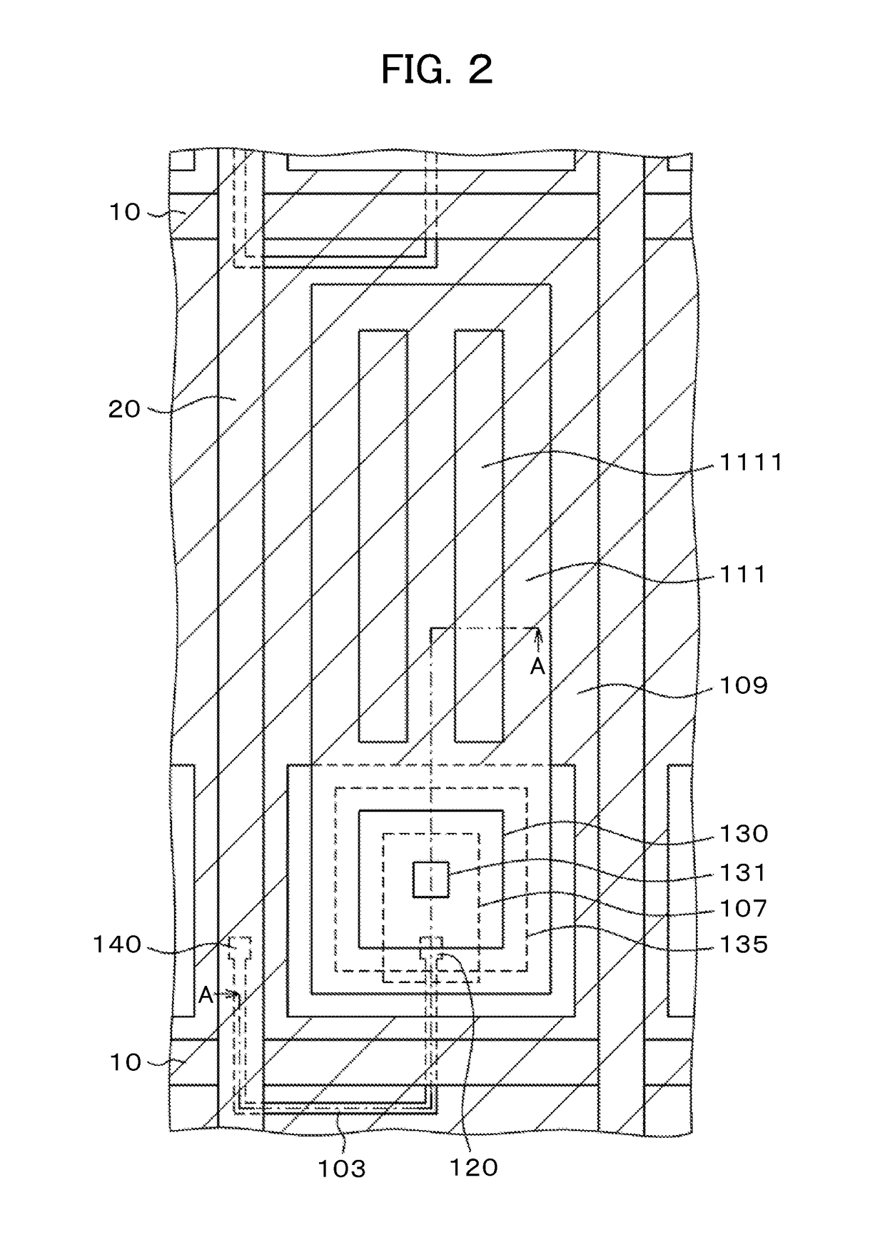
[0068]FIG. 9 is a plan view of the nearby area of the through-hole 130 according to Embodiment 2 of the invention. In terms of shape, FIG. 9 is the same as FIG. 7 that illustrates Embodiment 1. However, FIG. 9 differs from FIG. 7 in that, in the former, the connective electrode formed in the through-hole 130 is not formed of ITO but metal. This metal is hereinafter referred to as the connective metal 136. Since the common electrode 109 is formed across the entire screen except through-holes 130 and their nearby areas, increasing the thickness of the common electrode 109 will decrease the light transmittance, which may constitute a disadvantage in terms of screen brightness.

[0069]Therefore, it is desired that the common electrode 109 be formed thin. However, reducing the thickness of the common electrode 109 will, in turn, increase its electrical resistance when it is formed of ITO. To avoid this, metal wires are often formed on the common electrode 109. Such metal wires can be forme...

embodiment 3

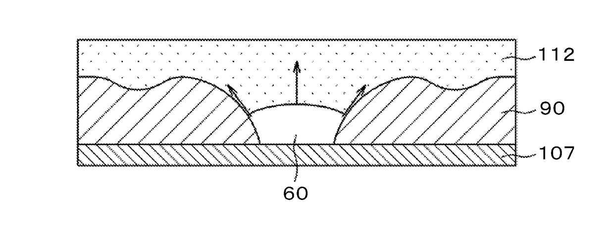
[0076]FIG. 11 is a cross section of the nearby area of the through-hole 130 according to Embodiment 3. A plan view of FIG. 11 is the same as that of FIG. 9. As illustrated in FIG. 11, the connective metal 136 is formed in and around the through-hole 130. The thickness of the connective metal 136 is, for example, about 150 nm, as is similar to Embodiment 2.

[0077]FIG. 11 differs from FIG. 10 in that, in the former, the thickness of the common electrode 109 is also increased as in Embodiment 1. Thus, the resultant recessed portion is allowed to have inner and outer steps of substantially the same height in a radial direction with respect to the center of the through-hole 130.

[0078]FIG. 11 also differs from FIG. 8 that illustrates Embodiment 1 in that, in the former, the distance w between the connective metal 136 and the common electrode 109 can be made smaller than the counterpart of Embodiment 1. The reason is the same as in Embodiment 2. Thus, the width of the black matrix can be ma...


PUM

PropertyMeasurementUnit
thicknessaaaaaaaaaa
heightaaaaaaaaaa
thicknessaaaaaaaaaa

Abstract

The invention prevents the display unevenness of a high-resolution liquid crystal display device that results from the presence of regions where an alignment film is not applied. The invention provides a liquid crystal display device including: a TFT substrate having scan lines, video signal lines, and pixels formed by the intersecting scan lines and video signal lines; a counter substrate; and a liquid crystal layer placed between the TFT substrate and the counter substrate. Each of the pixels includes a TFT, a pixel electrode, a common electrode, and a through-hole and an opening that are used to connect the TFT and the pixel electrode. Connective ITO is formed in and around the through-hole at the same time as the common electrode is formed. A step d is formed at an edge portion of the connective ITO and covered with an alignment film.

Description

CLAIM OF PRIORITY[0001]The present application claims priority from Japanese Patent Application JP 2016-157393 filed on Aug. 10, 2016, the content of which is hereby incorporated by reference into this application.BACKGROUND OF THE INVENTION1. Field of the Invention[0002]The present invention relates to display devices and particularly to a high-resolution liquid crystal display device that prevents display unevenness that results from the presence of regions where an alignment film is not formed.2. Description of the Related Art[0003]A typical liquid crystal display device includes a thin film transistor (TFT) substrate, a counter substrate facing the TFT substrate, and a liquid crystal layer placed between them. On the TFT substrate, pixels each having a pixel electrode, a TFT, and the like are formed in the form of a matrix. Images are produced by controlling the transmittance of light passing through the liquid crystal molecules on a pixel-by-pixel basis.[0004]On the TFT substra...

Claims


Application Information

Patent Timeline
Patent Type & Authority Applications(United States)
IPC IPC(8): G02F1/1337G02F1/1362G02F1/1343G02F1/1368
CPCG02F1/1337G02F1/1368G02F1/136286G02F1/136227G02F2201/121G02F1/136213G02F1/134363G02F2201/123G02F1/13439G02F1/134372
Inventor MIYAMOTO, MOTOHARU
Owner JAPAN DISPLAY INC
Why Eureka
Try Eureka