
Phased clock error handling

a phased clock and error handling technology, applied in pulse manipulation, pulse technique, instruments, etc., can solve the problems of serdes circuits even more attractive, deterministic jitter and/or other errors in the combined clock output, and increase power consumption, so as to improve the performance of voting and reduce the error range. , the effect of small resolution

Active Publication Date: 2017-08-03
ORACLE INT CORP
View PDF0 Cites 5 Cited by
  • Summary
  • Abstract
  • Description
  • Claims
  • Application Information

AI Technical Summary

Benefits of technology

This patent describes a system and method for detecting and correcting errors in clock signals used in electronic circuits. The system can detect errors in the output clock signal by measuring the width of the clock pulses and comparing them to a predetermined threshold. The system can then adjust the clock generation paths to correct the errors. This approach allows for accurate detection and correction of errors over a wide range of values and can improve performance by using voting and "ping-pong exiting" techniques.

Problems solved by technology

As bus speeds increase, parallel communications manifest even higher power consumption and more issues relating to timing (e.g., skew mismatches and bit misalignment), making SERDES circuits even more attractive.
However, slight differences between the multiple, separate, phased clocks (e.g., differences in their respective phase-locked loops, manufacturing variance, clock distribution, etc.) can cause deterministic jitter and / or other error in the combined clock output.
When four phased clocks are used, the clocks can be considered “quadrature clocks” and the error can be considered as “quadrature error.” or “QE.” For example, when such phased clocks are used for a SERDES transmission clock, particularly at very high data rates, the deterministic jitter (e.g., QE) can appreciably impact link performance.

Method used


Image

  • Phased clock error handling
  • Phased clock error handling
  • Phased clock error handling

Examples


Embodiment Construction

[0017]Many electronics applications include communications channels that have transmitter and receiver components to move data through the electronics application. Some transmitter (TX) circuits are serializer / deserializer (SERDES) TX circuits that can, for example, serialize differential data lines into a single, high-speed differential output, which can be fed through an equalizer (e.g., a finite impulse response (FIR) filter-based equalizer) that can shape the transmitted pulse to compensate for undesirable channel characteristics, such as frequency-dependent channel loss. High-performance processors and other applications often rely on very high data rates (e.g., 25 Gbps or higher), particularly when the data is serialized.

[0018]Achieving very high data rates can involve implementing vary fast clocking. However, very fast clock circuits can have undesirable operational characteristics, such as high power consumption and high complexity. Accordingly, some implementations use phas...


PUM


Abstract

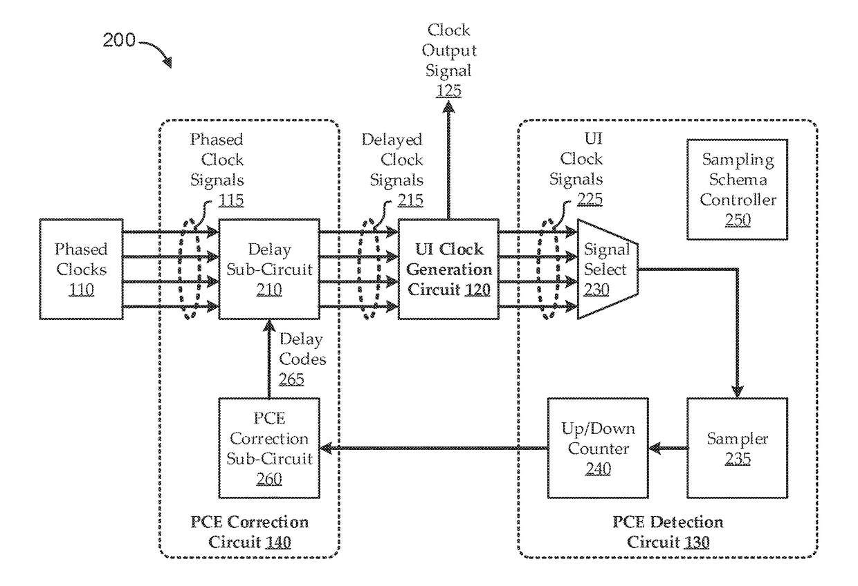
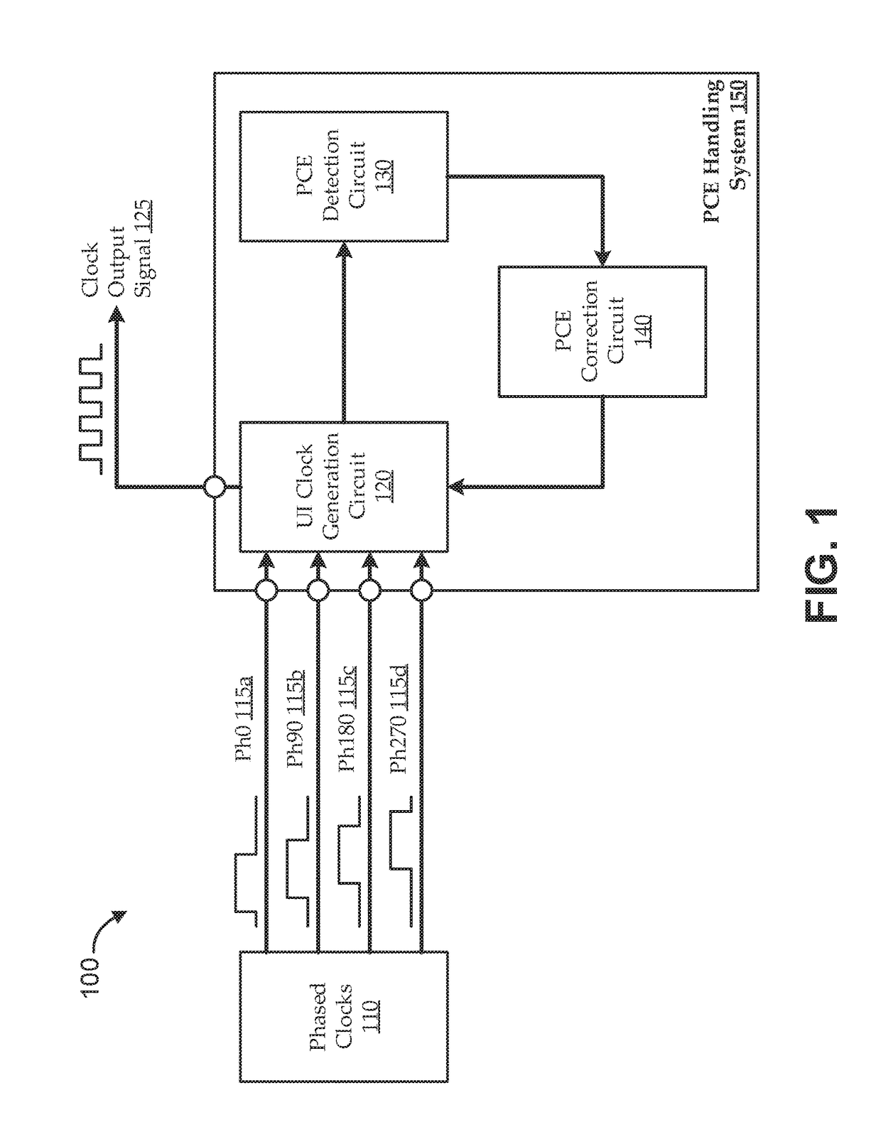
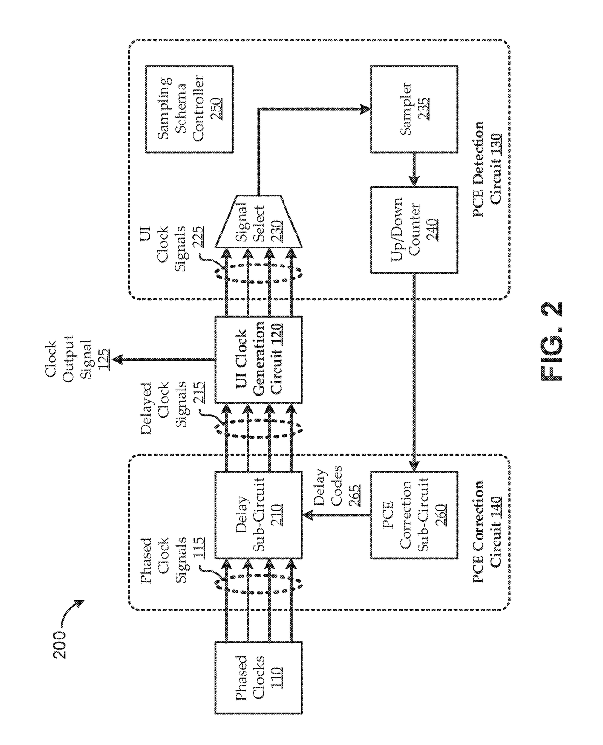
Embodiments include systems and methods for detecting and correcting phased clock error (PCE) in phased clock circuits (e.g., in context of serializer / deserializer (SERDES) transmission (TX) clock circuits). For example, phased input clock signals can be converted into unit interval (UI) clocks, which can be combined to form an output clock signal. PCE in the output clock signal can be detected by digitally sampling the UI clocks to characterize their respective clock pulse widths, and comparing the respective clock pulse widths (i.e., PCE in the output clock signal can result from pulse width differences in UI clocks). Delay can be applied to one or more UI clock generation paths to shift UI clock pulse transitions, thereby adjusting output clock pulse widths to correct for the detected PCE. Approaches described herein can achieve PCE detection over a wide error range and can achieve error correction with small resolution.

Description

FIELD[0001]Embodiments relate generally to clock circuits, and, more particularly, to techniques for detection and correction of error in phased clock circuits, such as quadrature clocks.BACKGROUND[0002]Serializer / deserializer (SERDES) circuits are becoming ubiquitous in many computational environments. The SERDES can compress a relatively wide, parallel input into a relatively narrow, serial signal (e.g., a single “bit,” differential signal) for communication over a serial bus. The serial bus switches at an appreciably higher rate than the parallel bus, and serial communication of the data stream tends to reduce cost, complexity, power, and board real estate relative to comparable parallel communications. As bus speeds increase, parallel communications manifest even higher power consumption and more issues relating to timing (e.g., skew mismatches and bit misalignment), making SERDES circuits even more attractive.[0003]Some SERDES applications use phased clocks to reduce power and ...

Claims


Application Information

Patent Timeline
Patent Type & Authority Applications(United States)
IPC IPC(8): H04L7/033
CPCH04L7/0337G01R25/005H03K5/151H03K5/1565H03K23/58H04L7/0025H04L7/0037
Inventor CHEN, BEN LIQIN, ZUXUEDELKHANI, NIMA
Owner ORACLE INT CORP
Learn More