Height measurement by correlating intensity with position of scanning object along optical axis of a structured illumination microscope

a structured illumination and height measurement technology, applied in the field of optical surface profilometry, can solve the problem of general limited lateral resolution of optical imaging systems

Active Publication Date: 2014-08-14
ACAD SINIC
View PDF2 Cites 5 Cited by
  • Summary
  • Abstract
  • Description
  • Claims
  • Application Information

AI Technical Summary

Benefits of technology

[0018]Among other advantages, the microscopy techniques described herein allow optical imaging and profilometry with a lateral resolution smaller than the optical diffraction limit and a depth profiling accuracy of less than 10 nm. Such high resolution is useful for a number of applications, including visualization of real-time biological processes and the imaging of complex nanostructures. These techniques can be implemented in a straightforward setup.

Problems solved by technology

However, the lateral resolution of optical imaging systems is generally limited by diffraction to about 0.5λ, where λ is the wavelength of the imaging light.

Method used


Image

  • Height measurement by correlating intensity with position of scanning object along optical axis of a structured illumination microscope
  • Height measurement by correlating intensity with position of scanning object along optical axis of a structured illumination microscope
  • Height measurement by correlating intensity with position of scanning object along optical axis of a structured illumination microscope

Examples


example 1

[0040]Referring to FIG. 3a, a SIM system was used to reconstruct an axially sectioned super-resolution image of a mesh pattern. A 100×, 1.1 NA water-immersion objective with a lateral resolution of 260 nm at an illumination wavelength of 475 nm was used.

[0041]An electron-multiplying CCD camera captured the resulting images. A mesh pattern was projected onto a reflective mirror, generating a pattern with a period of 0.5 μm on the mirror surface. The mesh pattern was placed at five different positions, each position having a different modulated intensity I and phase Φx, Φy, generating five images I0-I4. A super-resolution image was reconstructed from the five images using an image processing algorithm. The mirror was then scanned along the z-axis of the SIM system (i.e., along the axis of the illumination light).

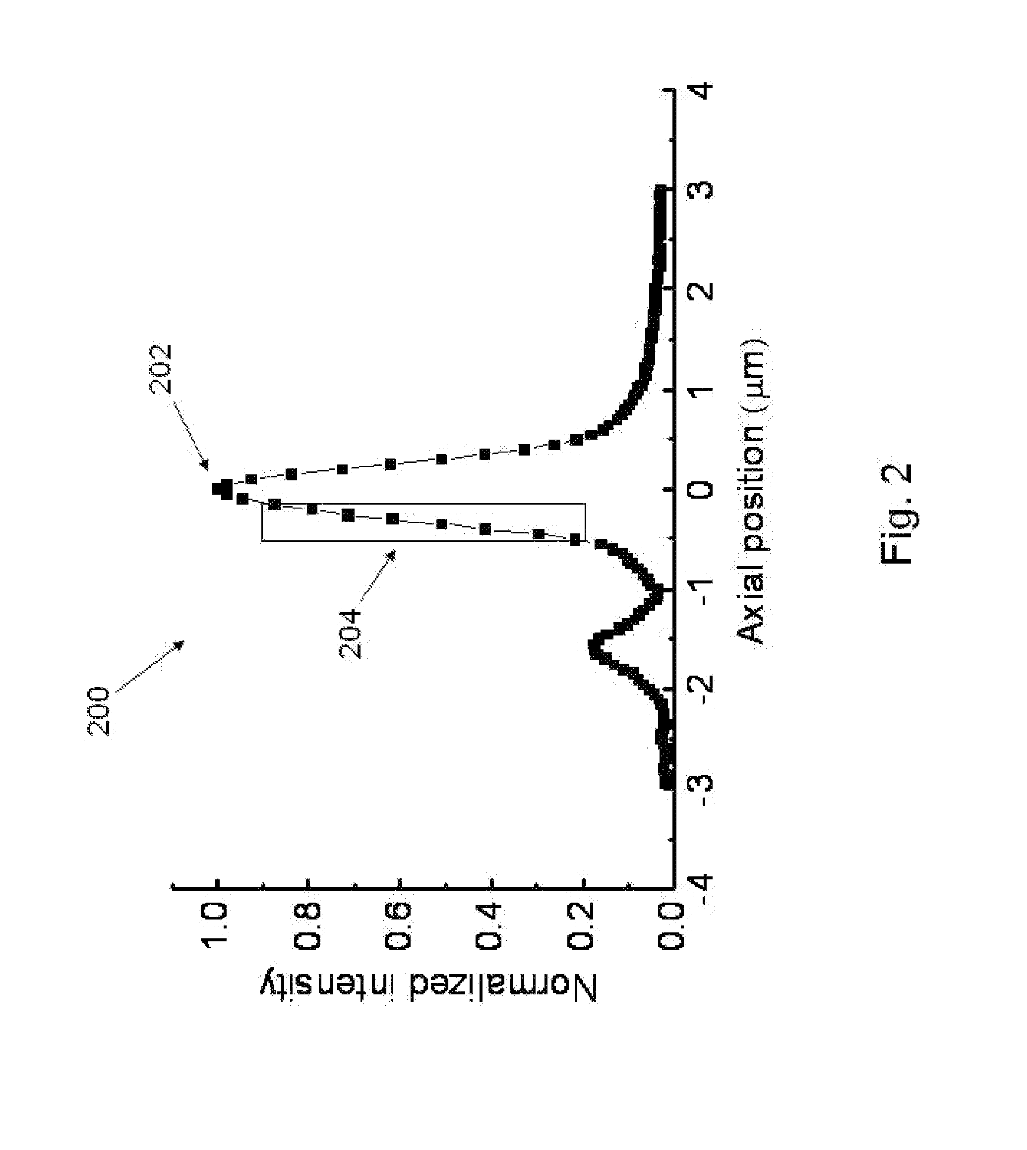
[0042]Super-resolution images were reconstructed as described above for seven height positions of the minor. Referring to FIG. 3b, a linear relationship is seen between the he...

example 2

[0043]Referring to FIGS. 4a and 4b, a conventional bright-field microscopy image of four 80 nm gold particles on a glass substrate and a corresponding super-resolution image obtained by SIM are shown. The surface of the glass substrate was placed at the focal plane of the SIM to demonstrate the bright-field super-resolution capability.

[0044]Referring to FIG. 4c, line profiles corresponding to the dashed white lines in FIGS. 4a (gray curve) and 4b (black curve) are shown. An intensity dip is observed in the profile obtained from the SIM image, indicating that two adjacent 80 nm particles can be resolved using SIM. Conventional bright-field microscopy does not resolve the two adjacent particles.

[0045]The Airy formula, I(r)=[2J1(r) / r]2, where J1 is the 1st order Bessel function of the first kind, is used to estimate the distance between the two particles. The intensity dip can be fitted by the summation of two Airy formulas of 175 nm width (FWHM) and separated by 190 nm. The summation ...

example 3

[0046]A gold wire is used to demonstrate the depth profiling accuracy of SIM. This wire was fabricated by using electron-beam lithography and a lift-off process on a silicon substrate. Referring to the AFM topography image in FIG. 5a, the width and height of the wire are 450 nm and 115 nm, respectively. A conventional bright-field image of the wire, shown in FIG. 5b, gives a width of about 770 nm due to diffraction effects. The edge response from 10% to 90% of the intensity variation on the wire is about 240 nm, close to the optical resolution of the objective (260 nm). The scattering from the edges of the wire makes a dark outline in the bright-field image. The effect of scattering or inhomogeneous reflectivities can be removed by dividing image intensity obtained in the linear region of the axial response curve with the image intensity obtained on the focal plane.

[0047]After the calibration of the signal intensity to the height variations, the super-resolution topography of the go...


PUM


Abstract

A method for imaging an object using a microscope includes obtaining axial response data, the axial response data representative of a relationship between a separation between a top surface of the object and an objective lens of the microscope and an intensity of light reflected by the top surface of the object; positioning the object at a distance from the objective lens that is within a linear region of the axial response data; sequentially illuminating the object with a plurality of periodic patterns; obtaining a plurality of images of the object, each image resulting from the illumination of the object with a corresponding one of the plurality of periodic patterns; determining a reconstructed image of the object based on the plurality of images of the object; and, based on variations in the intensity of the reconstructed image, determining a topographic profile of the top surface of the object.

Description

CROSS-REFERENCE TO RELATED APPLICATIONS[0001]The present application is a divisional of commonly assigned copending U.S. patent application Ser. No. 12 / 966,207, which was filed on Dec. 13, 2010, by Chau-Hwang Lee for a HEIGHT MEASUREMENT BY CORRELATING INTENSITY WITH POSITION OF SCANNING OBJECT ALONG OPTICAL AXIS OF A STRUCTURED ILLUMINATION MICROSCOPE and is hereby incorporated by reference.[0002]The present application is related to the following commonly assigned U.S. Provisional Patent Application Ser. No. 61 / 286,098, which was filed on Dec. 14, 2009, by Chau-Hwang Lee for a OPTICAL PROFILOMETRY and is hereby incorporated by reference.BACKGROUND OF THE INVENTION[0003]1. Field of the Invention[0004]This invention relates to optical surface profilometry.[0005]2. Background Information[0006]High resolution surface profilometry plays an important role in nanoscience and biological research. For instance, atomic force microscopy (AFM) can be used to study biomolecular activities in r...

Claims


Application Information

Patent Timeline
Patent Type & Authority Applications(United States)
IPC IPC(8): G01B11/25G01B11/06
CPCG01B11/0608G01B11/25G06T2207/10016G06T2207/10056G06T2207/30004G06T7/521
Inventor LEE, CHAU-HWANGWANG, CHUN-CHIEH
Owner ACAD SINIC
Why Eureka
Try Eureka