Device for jitter measurement and method thereof

a jitter measurement and device technology, applied in the direction of noise figure or signal-to-noise ratio measurement, transmission monitoring, instruments, etc., can solve the problems of reducing system reliability, reducing measurement accuracy, and inconvenient operation of data transmission, so as to reduce the load effect, reduce the size of the chip area, and reduce the effect of jitter

Active Publication Date: 2011-06-07
HIMAX TECH LTD +1
View PDF4 Cites 6 Cited by
  • Summary
  • Abstract
  • Description
  • Claims
  • Application Information

AI Technical Summary

Benefits of technology

[0010]Accordingly, the present invention provides a device for jitter measurement and a method thereof. The measuring device and method have several advantages, such as small resolution, multiple resolutions, and no needs of the reference signals. Furthermore, the measuring device for built-in self testing can save the chip area and alleviate load effect.
[0011]A device for jitter measurement is provided in the present invention. The device for jitter measurement includes a signal retrieving module, a signal amplifying module, an edge detecting module, and a time-to-digital converting module. The signal retrieving module receives a signal-under-test, and outputs a first pulse signal having a pulse width equal to a period of the signal-under-test. The signal amplifying module amplifies the pulse width of the first pulse signal for equivalently improving the resolution of the first pulse signal, and thereby generates a second pulse signal. The edge detecting module respectively detects a rising edge and a falling edge of the second pulse signal, and generates a first indication signal and a second indication signal. The time-to-digital converting module converts the pulse width of the second signal existed in time domain to a digital signal according to the first indication signal and the second indication signal.
[0013]The present invention provides a device for jitter measurement and a method thereof that amplifies the pulse width of the first pulse signal to equivalently improve the resolution for measuring the jitter value. Therefore, by adjusting different amplifying ratios, the jitter value of the signal-under-test can be quantified by multiple resolutions. The second pulse signal is obtained by amplifying the first pulse signal, and the first indication signal and the second indication signal are obtained by respectively detecting the rising edge and the falling edge of the second pulse signal. The pulse width of the second pulse signal existed in time domain can be converted to a digital signal by the time-to-digital converting module according to the first and the second indication signals so as to obtain the jitter value of the signal-under-test.

Problems solved by technology

As for a data transmission system, jitter would cause the incorrect operation of data transmission, and reduce the system reliability even cause error operation of the system.
However, the input and output (I / O) pads and bonding wirings often distort the output signal of the chip and reduce the accuracy of measuring results.
Nevertheless, the number of pins has not increased nearly as fast as the number of transistors due to mechanical limitation of the packaging technology.
As a result, the pins that can be provided for testing are limited, and not all the signals-under-test (SUTs) can be accessed through independent pins.
Nevertheless, the serial transmission can not be applied to the analog signal.
The limit of pin counts and the unpredictable characteristic in transmitting the on-chip signal-under-test increase the testing difficulties of mix-signal chips.
The most important issue of the jitter measurement method by built-in self testing is to convert the continuous-time signal to a digital representation for the convenience of reading out and further processing.
Although, the resolution which is less than the delay time of a logic gate for jitter measurement is achieved in the said article, the ring oscillators 130 and 140 may produce unwanted noises, and the delay time is not easy to control due to the affection of process variation and operation environment.

Method used


Image

  • Device for jitter measurement and method thereof
  • Device for jitter measurement and method thereof
  • Device for jitter measurement and method thereof

Examples


Embodiment Construction

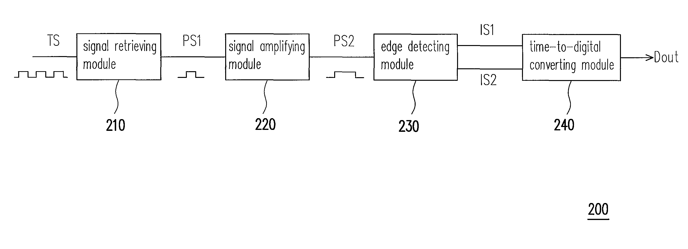
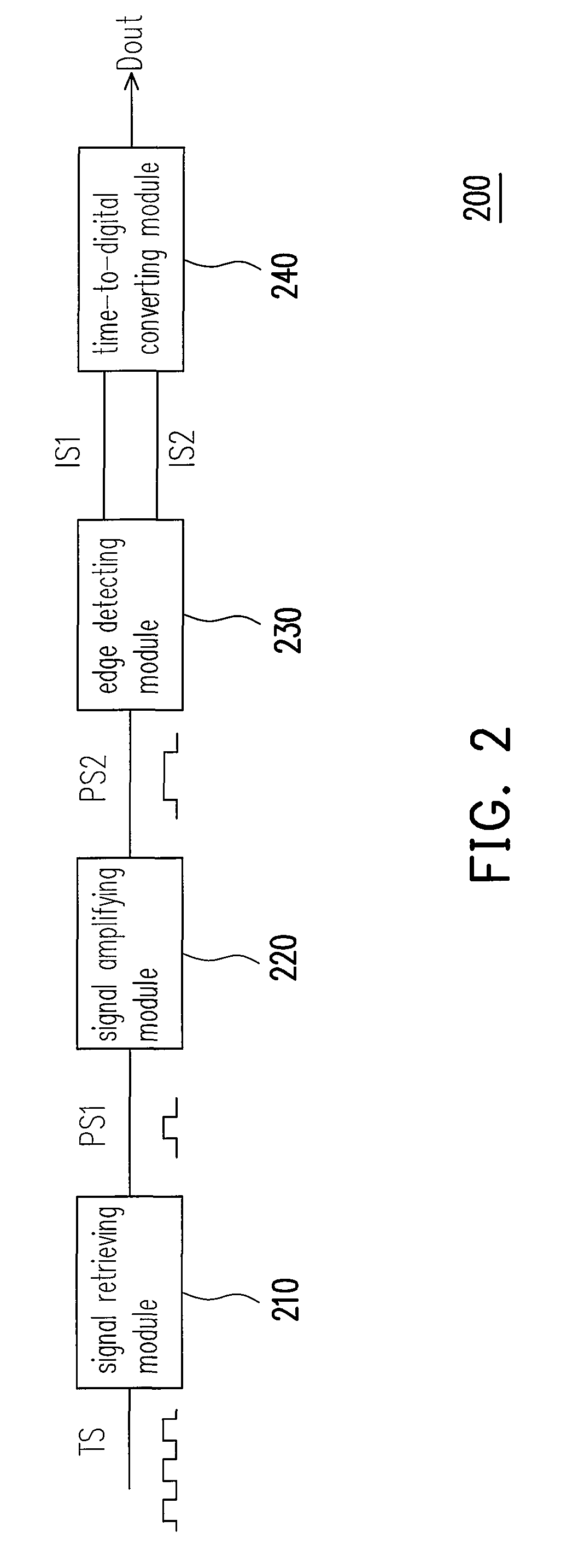
[0028]FIG. 2 is a block diagram of a device for the jitter measurement according to an embodiment of the present invention. Referring to FIG. 2, the device 200 for jitter measurement includes a signal retrieving module 210, a signal amplifying module 220, an edge detecting module 230 and a time-to-digital converting module 240. The signal retrieving module 210 receives a signal-under-test TS and retrieves a first pulse signal PS1 having a pulse width equal to a period of the signal-under-test TS. The signal amplifying module 220 amplifies the pulse width of the first pulse signal PS1 and thereby generates a second pulse signal PS2. Since the pulse width of the first pulse signal PS1 is one period length of the signal-under-test TS in time domain, amplifying the pulse width of the first pulse signal PS1 equivalently improves the resolution of the first pulse signal PS1. The edge detecting module 230 detects a rising edge and a falling edge of the second pulse signal PS2 and thereby g...


PUM


Abstract

The device for jitter measurement and a method thereof are provided. The device for jitter measure includes a signal retrieving module, a signal amplifying module, an edge detecting module, and a time-to-digital converting module. The signal retrieving module receives a signal-under-test, and retrieves a first pulse signal having a pulse width equal to a period of the signal-under-test. The signal amplifying module amplifies the pulse width of the first pulse signal and thereby generates a second pulse signal. The edge detecting module detects a rising edge and a falling edge of the second pulse signal, and generates a first indication signal and a second indication signal according to the respective detected results. The time-to-digital converting module converts the pulse width of the second pulse signal existed in time domain to a digital signal according to the first indication signal and the second indication signal.

Description

CROSS-REFERENCE TO RELATED APPLICATION[0001]This application claims the priority benefit of U.S.A. provisional application Ser. No. 60 / 949,879, filed on Jul. 16, 2007. The entirety of the above-mentioned patent application is hereby incorporated by reference herein and made a part of specification.BACKGROUND OF THE INVENTION[0002]1. Field of the Invention[0003]The present invention relates to a device for jitter measurement and method thereof, and more particularly, to a device and a method that utilize the delay lines to implement the jitter measurement.[0004]2. Description of Related Art[0005]Jitter is a time shifting interval of a signal between a real transition location and an ideal transition location. As for a data transmission system, jitter would cause the incorrect operation of data transmission, and reduce the system reliability even cause error operation of the system. Jitter analysis has become more important in recent years due to high speed data calculation and signal...

Claims


Application Information

Patent Timeline
Patent Type & Authority Patents(United States)
IPC IPC(8): G06F19/00H04B3/46
CPCG01R31/31709
Inventor CHAO, AN-SHENGCHANG, SOON-JYHHUANG, CHIH-HAURHUANG, KUO-CHANLUO, SHIH-MING
Owner HIMAX TECH LTD
Why Eureka
Try Eureka