Method of manufacturing support structures for lighting devices and corresponding device

a technology for supporting structures and lighting devices, applied in the field of manufacturing support structures for lighting devices and corresponding devices, can solve the problems of reducing the resolution of lines or tracks, increasing costs and lead time, and long manufacturing times, and achieves the effect of reducing manufacturing times and high customization degr

Active Publication Date: 2018-03-01
OPTOTRONIC GMBH
View PDF4 Cites 4 Cited by
  • Summary
  • Abstract
  • Description
  • Claims
  • Application Information

AI Technical Summary

Benefits of technology

[0022]One or more embodiments may envisage different solutions, the possibility being given of implementing FPCB components having a high customization degree, by resorting either to single-sided or to double-sided clad substrates.
[0023]In one or more embodiments it is possible to employ hybrid techniques, which may be defined in the final product with possible reductions of manufacturing times.

Problems solved by technology

FPCB boards may include laminates of metal materials such as copper or aluminium (either single- or double-sided) which may require, in order to achieve a given circuit arrangement, various chemical processes as well as, in some cases, a specific machining, leading to rather long manufacturing times.
This solution, however, suffers from a drawback: in order to change the circuit layout, it may be necessary to completely redesign the FPCB support, possibly entailing the intervention of the component manufacturer, with a consequent increase in costs and lead time.
Moreover, the thickness of said conductive layer (e.g. of copper or aluminium) is usually standardized and limited to certain values, such as e.g. 35 μm, 75 μm and 105 μm (1 μm=10−6 m), the presence of rather large thicknesses being prone to reduce the resolution of the lines or tracks, which may lead to a limitation regarding the possible use of small-sized (e.g. LED) components.
In a complementary way, rather wide lines or tracks may lead to an increase of the width of the product as a whole, which may represent a disadvantage in various applications.

Method used


Image

  • Method of manufacturing support structures for lighting devices and corresponding device
  • Method of manufacturing support structures for lighting devices and corresponding device
  • Method of manufacturing support structures for lighting devices and corresponding device

Examples


Embodiment Construction

[0038]In the following description, various specific details are given to provide a thorough understanding of various exemplary embodiments. The embodiments may be practiced without one or more specific details, or with other methods, components, materials, etc. In other instances, well-known structures, materials or operations are not shown or described in detail to avoid obscuring various aspects of the embodiments.

[0039]Reference throughout this specification to “one embodiment” or “an embodiment” means that a particular feature, structure, or characteristic described in connection with the embodiment is included in at least one embodiment. Thus, the possible appearances of the phrases “in one embodiment” or “in an embodiment” in various places throughout this specification are not necessarily all referring to the same embodiment. Furthermore, particular features, structures, or characteristics may be combined in any suitable manner in one or more embodiments.

[0040]The headings p...


PUM

PropertyMeasurementUnit
thicknessesaaaaaaaaaa

Abstract

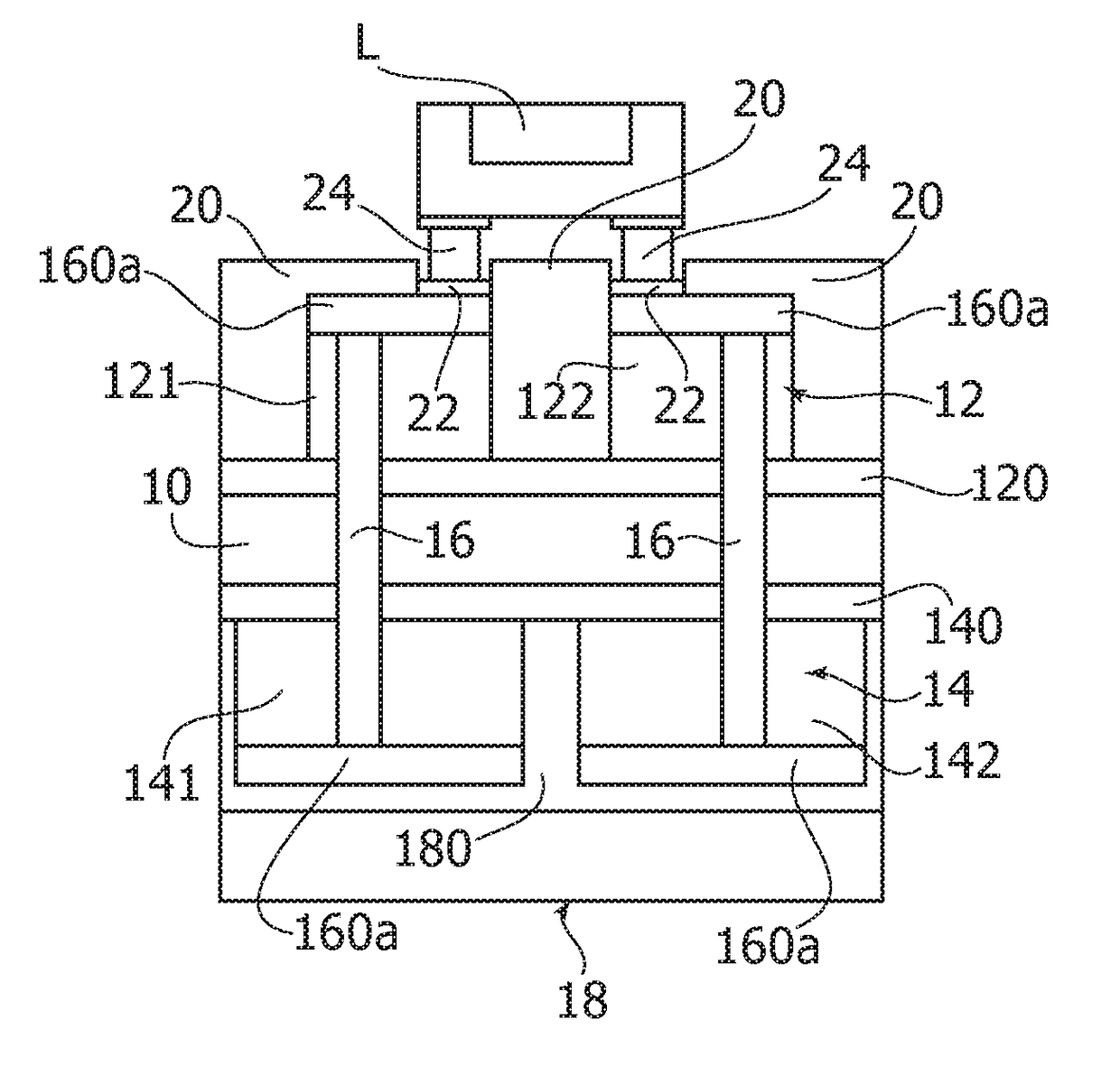
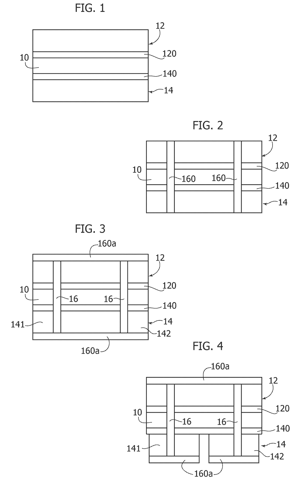
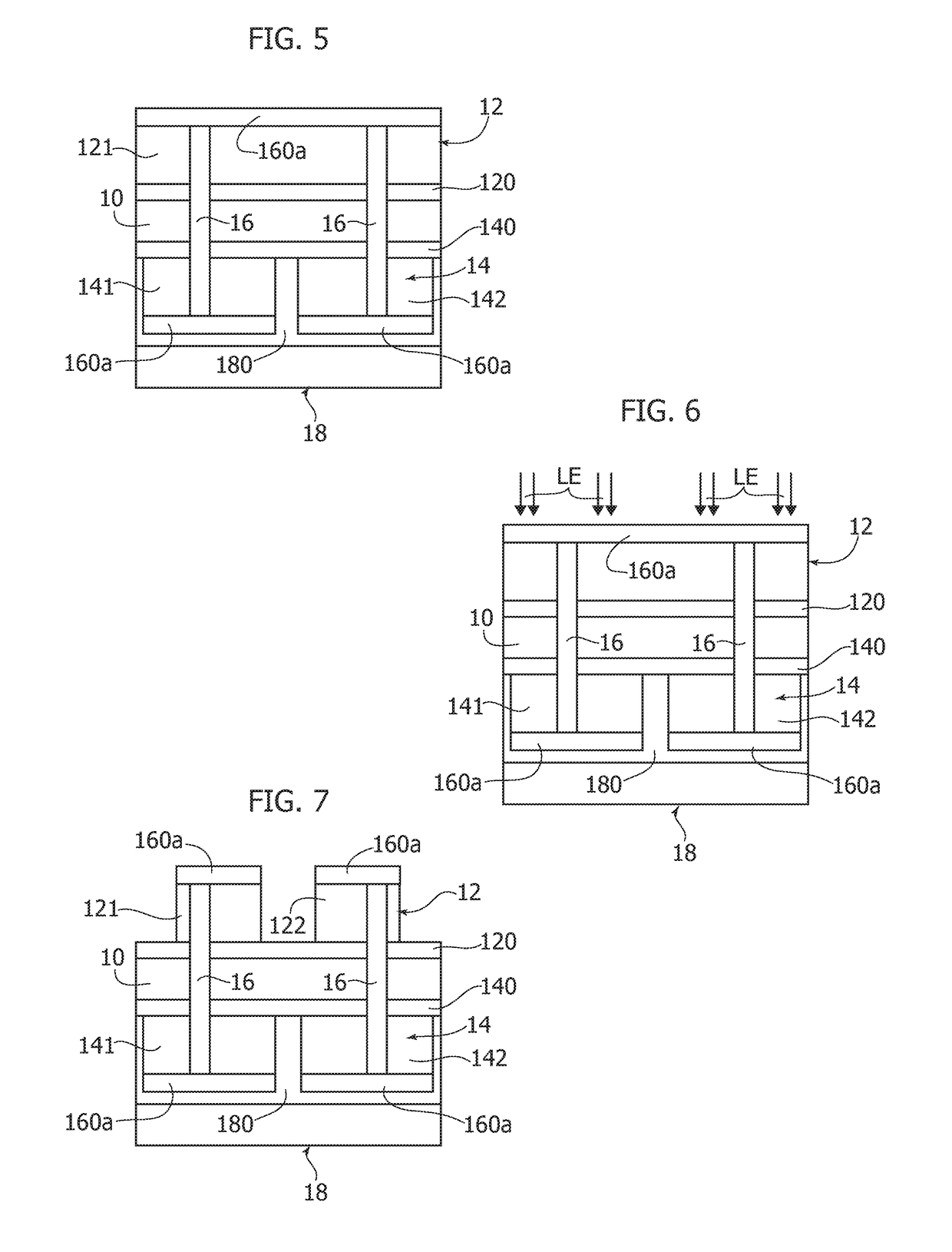
A method of manufacturing support elements for lighting devices includes: providing an elongated, electrically non-conductive substrate with opposed surfaces, with an electrically-conductive layer extending along one of said opposed surfaces, etching said electrically-conductive layer to provide a set of electrically-conductive tracks extending along the non-conductive substrate with at least one portion of the non-conductive substrate left free by the set of electrically-conductive tracks, forming a network of electrically-conductive lines coupleable with at least one light radiation source at said portion of said non-conductive substrate left free by the electrically-conductive tracks. Said forming operation includes selectively removing e.g. via laser etching a further electrically-conductive layer provided on said non-conductive substrate, or printing electrically-conductive material onto the non-conductive substrate. The electrically-conductive tracks and the network of electrically-conductive lines may be coupled with each other e.g. by means of electrically-conductive vias extending through the non-conductive substrate.

Description

CROSS-REFERENCE TO RELATED APPLICATION[0001]This application claims priority to Italian Patent Application Serial No. 102016000088158, which was filed Aug. 30, 2016, and is incorporated herein by reference in its entirety.TECHNICAL FIELD[0002]The description relates to lighting devices.[0003]One or more embodiments may refer to lighting devices employing electrically-powered light radiation sources, e.g. solid-state light radiation sources, such as LED sources.BACKGROUND[0004]The field of lighting technology, e.g. in Solid State Lighting (SSL), increasingly demands lighting modules, e.g. LED modules, with short development and lead times.[0005]The linear and flexible (“flex”) LED modules which are employed nowadays may include a plurality of electrical units which are connected e.g. in parallel (and which include one or more LED strings or chains and the related driving circuitry) with a consequent increase of the supply currents delivered along the module.[0006]This fact may affect...

Claims


Application Information

Patent Timeline
Patent Type & Authority Applications(United States)
IPC IPC(8): H01L33/62H05K3/18H05K3/24H05K3/42F21K9/90F21V19/00F21V23/00H01L33/00H01L33/48
CPCH01L33/62H05K3/184H05K3/242H05K3/428F21Y2115/10F21V19/005F21V23/005H01L33/005H01L33/483F21K9/90H05K1/095H05K1/189H05K3/027H05K3/06H05K3/12H05K2201/0154H05K2201/10106H05K2203/107H05K5/06
Inventor BALDO, LORENZOGRIFFONI, ALESSIOPOGGI, FEDERICO
Owner OPTOTRONIC GMBH
Why Eureka
Try Eureka