Method for operation of a field effect transistor arrangement

a field effect transistor and arrangement technology, applied in the direction of transistors, semiconductor devices, electrical equipment, etc., can solve the problems of high cost, high complexity, power loss and heat that must be dissipated, etc., to achieve short switching times, high switching speeds, and the effect of reducing the distance between the control electrode and the underside of the planar channel layer

Inactive Publication Date: 2018-03-15
TECH UNIV DARMSTADT
View PDF1 Cites 0 Cited by
  • Summary
  • Abstract
  • Description
  • Claims
  • Application Information

AI Technical Summary

Benefits of technology

[0007]With some known field effect transistor arrangements, their characteristics, for example the majority charge carrier type, can be influenced even after the field effect transistor arrangement has been produced. Ambipolar field effect transistors are known from practice, in which the current of the transistor that is available for applications can be generated and sustained both by electrons and by defect electrons. Recent developments along these lines relate, for example, to finFETs or “nanowire” structures, in which the charge carrier channel extends substantially unidimensionally in one direction and the control electrode encompasses the charge carrier channel on as many sides as possible. The substantially unidimensional configuration of the charge carrier channel and the small dimensions thereof allow rapid switching times and low power losses during switching processes to be achieved. However producing such field effect transistor arrangements is highly complex and costly.
[0028]According to the invention, complex circuits can be easily and cost-efficiently produced by arranging a plurality of planar channel layers consisting of or comprising a semiconductor material, each with respectively assigned source electrodes, drain electrodes, control electrodes and adjusting electrodes, side by side on a common carrier substrate and separating them from one another by vertical trenches or insulators. With such an arrangement of a large number of field effect transistors having the above-described features and characteristics, reconfigurable circuits can also be produced, for example, in which a small space requirement can be combined with short switching times and low power losses. Each planar channel layer can be concentrated with electrons or with electron defects as majority charge carriers, depending on the actuation of the assigned adjusting electrode, and can therefore be used as an n-channel transistor or as a p-channel transistor. It is not necessary to provide respective stationary n-channel transistors and p-channel transistors when producing complex circuits.

Problems solved by technology

Producing complex circuits using such small transistors is costly and prone to errors.
Even if the switching state of a transistor is not changed, the leakage currents, which are nearly unavoidable particularly with small dimensions, generate power losses and heat that must be dissipated to keep the field effect transistors twin overheating.
However producing such field effect transistor arrangements is highly complex and costly.

Method used


Image

  • Method for operation of a field effect transistor arrangement
  • Method for operation of a field effect transistor arrangement
  • Method for operation of a field effect transistor arrangement

Examples


Embodiment Construction

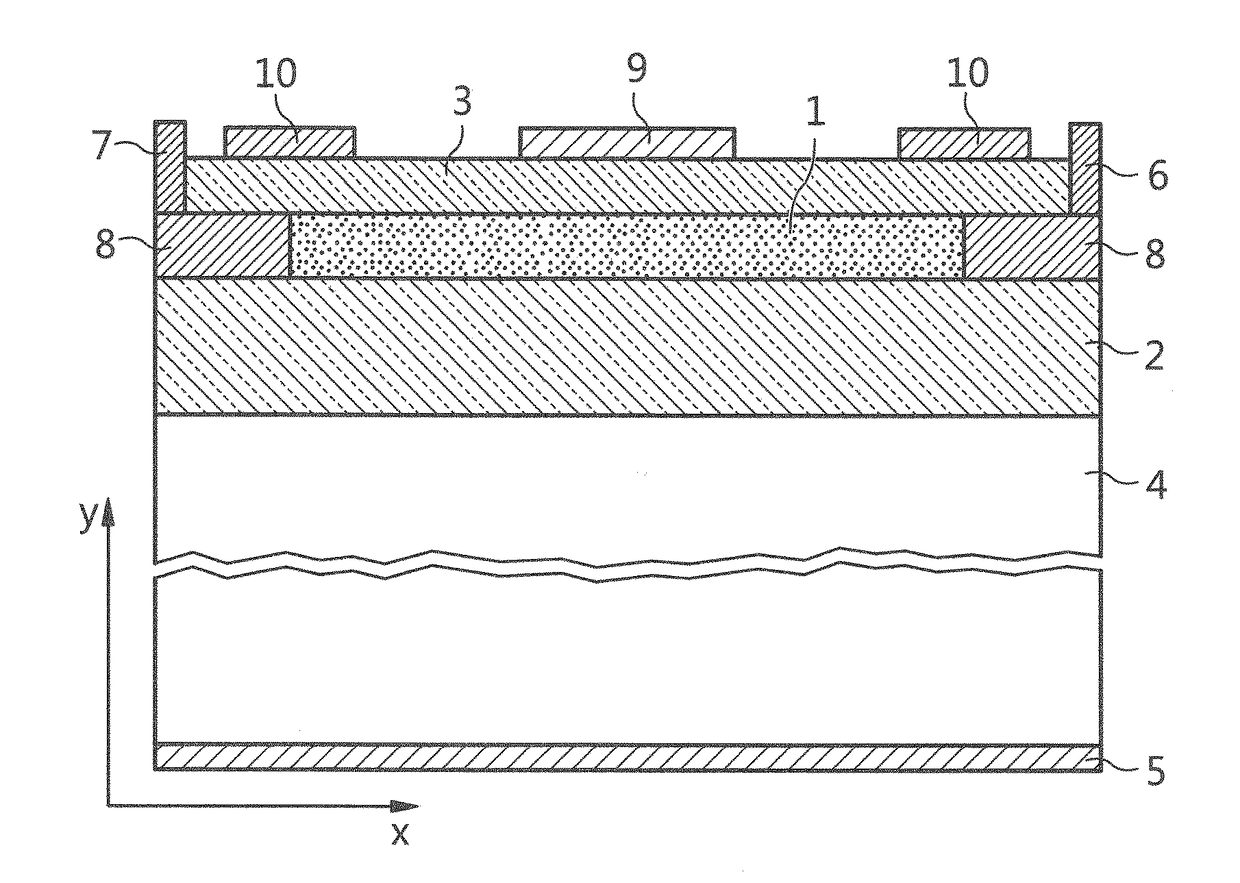
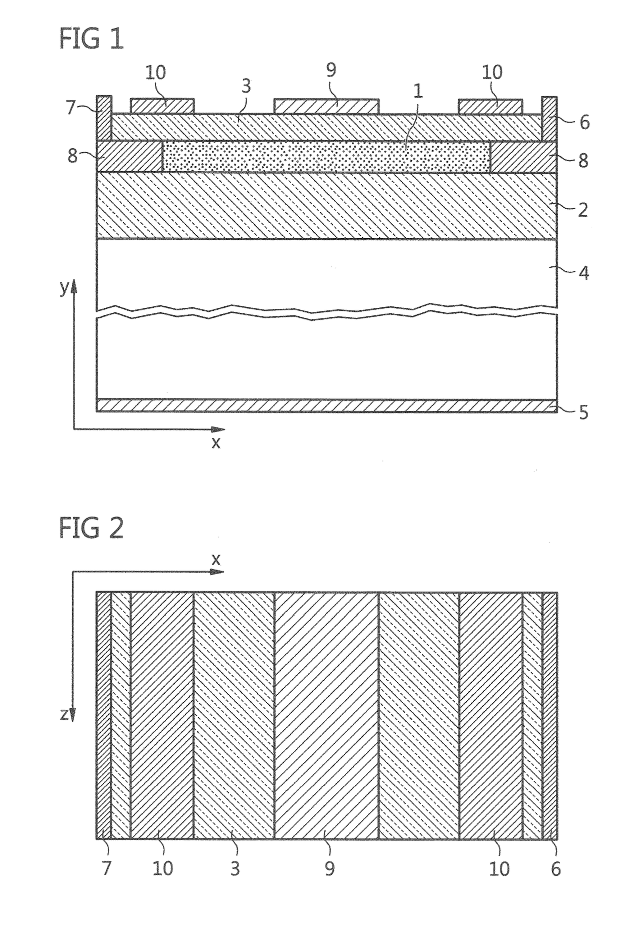
[0047]A field effect transistor arrangement schematically illustrated in FIGS. 1 and 2 has a planar channel layer 1 made of an undoped silicon material. The planar channel layer 1 is arranged on an upper side of an electrically insulating substrate layer 2, which consists of or comprises silicon oxide. The planar channel layer 1 is covered by an electrically insulating electrode insulation layer 3, which likewise consists of or comprises silicon oxide. Below substrate layer 2 a carrier substrate 4, and on the entire surface of the underside thereof, an electroconductively contactable adjusting electrode 5 are arranged.

[0048]On two opposite side edges of planar channel layer 1, an electroconductively contactable source electrode 6 and a drain electrode 7 are arranged, which protrude through electrode insulation layer 3, each into a contact region 8 that borders the planar channel layer laterally. Contact region 8 is embodied as a midgap Schottky barrier and is produced from nickel si...


PUM


Abstract

A method is provided for operation a field effect transistor arrangement, the field effect transistor arrangement having a planar channel layer including a semiconductor material, a whole surface of an underside of the planar channel layer being applied to a top side of an electrically insulating substrate layer and an upper side of the planar channel layer being covered by an electrically insulating electrode insulation layer, the arrangement having a source electrode disposed by a first side edge of the planar channel layer and having a drain electrode disposed by a second side edge of the planar channel layer, and having a control electrode arranged above the planar channel layer between the source electrode and the drain electrode, wherein an adjusting electrode is arranged on an underside of the substrate layer, and a first contact region between the source electrode and the planar channel layer and a second contact region between the drain electrode and the planar channel layer are each a Schottky barrier, wherein a respective barrier control electrode is arranged between the first contact region of the source electrode and the control electrode and between the second contact region of the drain electrode and the control electrode, the method including providing a first electric potential to the control electrode, providing a second electric potential to the barrier electrodes, and providing a third electric potential to the adjusting electrode.

Description

BACKGROUND AND SUMMARY[0001]The present application is a continuation of U.S. application Ser. No. 14 / 900,704, filed Dec. 22, 2015, which is the U.S. national stage of PCT / EP2014 / 063459, tiled Jun. 25, 2014, which claims priorirty to DE 10 2013 106 729.8, filed Jun. 26, 2013, all of which are incorporated by reference.[0002]The invention relates to a field effect transistor arrangement having a planar channel layer consisting of or comprising a semiconductor material, the whole surface of the underside of said layer being applied to an upper side of an electrically insulating substrate layer, and the upper side of said planar channel layer being covered by an electrically insulating electrode insulation layer, said arrangement also having a source electrode on a first side edge of the channel layer and a drain electrode on a second side edge of the channel layer, and having a control electrode arranged above the channel layer between the source electrode and the drain electrode.[000...

Claims


Application Information

Patent Timeline
Patent Type & Authority Applications(United States)
IPC IPC(8): H01L29/78H01L29/40H01L29/06H01L29/786
CPCH01L29/7838H01L29/404H01L29/0649H01L29/7839H01L29/78648H01L29/78645H01L29/78654
Inventor SCHWALKE, UDOWESSELY, FRANKKRAUSS, TILLMANN
Owner TECH UNIV DARMSTADT
Why Eureka
Try Eureka