
Stacked-filter image-sensor spectrometer and associated stacked-filter pixels

a technology of imagesensor and spectrometer, which is applied in the field of stacking filter imagesensor spectrometer and associated stacking filter pixels, can solve the problems of spectrometer cost, spectrometer size and cost, and spectrometer cost remains high

Inactive Publication Date: 2018-03-22
OMNIVISION TECH INC
View PDF2 Cites 7 Cited by
  • Summary
  • Abstract
  • Description
  • Claims
  • Application Information

AI Technical Summary

Benefits of technology

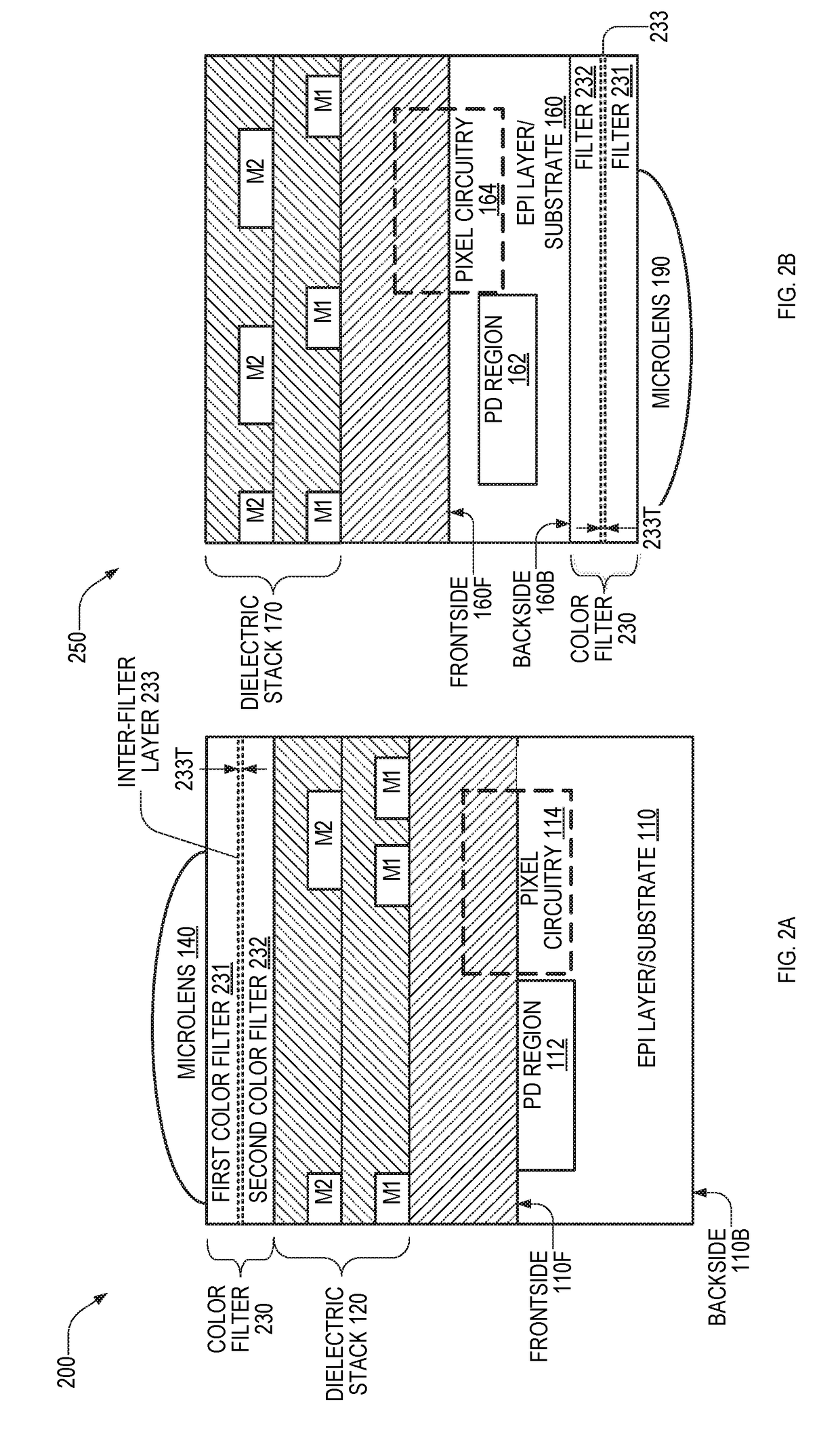
This patent describes a type of pixel structure called a stacked-filter pixel, which has a color filter stack with two color filters and an inter-filter layer between them. The inter-filter layer is transparent to the second filter, which allows for partial overlap between the two filters in a specific range. Another embodiment is a stacked-filter image-sensor spectrometer, which includes an image sensor and two color filter arrays. Each pixel has a compound color filter formed by one of the two color filters and one of the first filters. The second filter has a passband that partially overlaps the first filter's passband in a specific range. The technical effect of this patent is the creation of a more complex and versatile pixel structure for image sensors that can capture more information about the surrounding environment, leading to improved quality of captured images.

Problems solved by technology

A limitation to this technology is spectrometer size and cost.
Spectrometer size needs to exceed a volume required to accommodate both this light dispersion and the light dispersion system itself, which also contributes to spectrometer cost.
However, fabricating SPP-based metallic-dielectric filters requires a complex wafer manufacturing process so spectrometer cost remains high.

Method used


Image

  • Stacked-filter image-sensor spectrometer and associated stacked-filter pixels
  • Stacked-filter image-sensor spectrometer and associated stacked-filter pixels
  • Stacked-filter image-sensor spectrometer and associated stacked-filter pixels

Examples


Embodiment Construction

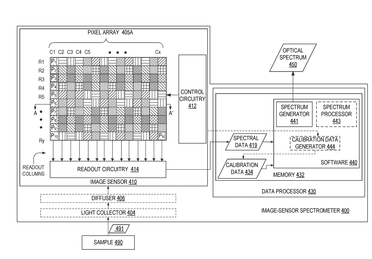
[0012]In the present disclosure, a stacked filter image-sensor spectrometer uses a multi-layer stacked color filter to select a relatively narrow wavelength band for detection. The color filter works by light absorption, and is fabricated with standard photolithography processes. Cost of the final spectrometer product is accordingly low as compared to the prior art.

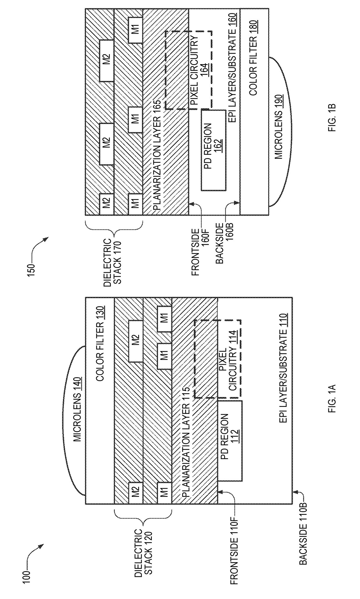
[0013]FIG. 1A illustrates a cross-section of an embodiment of a frontside-illuminated (FSI) pixel 100 in a solid state optical detection device based on CMOS image sensor pixel architecture. FSI pixel 100 includes a substrate 110 upon which a photodiode region 112 and associated pixel circuitry 114 are formed, and over which a dielectric stack 120 is formed. Dielectric stack 120 includes metal layers M1 and M2 for redistributing electrical signals. Metal layers M1 and M2 are patterned to allow optical passage of light incident on FSI pixel 100 to photodiode regions 112. A planarization layer 115 is between substrate 110 a...


PUM


Abstract

A stacked-filter image-sensor spectrometer includes an image sensor, a first color filter array, and a second color filter array. The image sensor has a pixel array including a plurality of pixels. The first color filter array has a plurality of first color filters, wherein each first color filter is located above at least one pixel. The second color filter array is located between the first color filter array and the image sensor and has a plurality of second color filters. Each second color filter is located above at least one pixel. Each of the plurality of pixels has thereabove a compound color filter formed of one of the second color filters and one of the first color filters, the second filter having a second passband that partially overlaps a first passband of the first color filter in a first overlapping wavelength range.

Description

BACKGROUND[0001]Optical spectroscopy has been widely used to detect and quantify characteristics and concentrations of physical, chemical, or biological targets. A limitation to this technology is spectrometer size and cost. More specifically, spectrometers traditionally use a light dispersion method. A light dispersion system, which may include a prism or diffraction grating, disperses incoming light from a target sample into an optical spectrum, i.e., into components of different wavelengths. This optical spectrum is then scanned by an optical detector to investigate the spectral characteristics. Spectrometer size needs to exceed a volume required to accommodate both this light dispersion and the light dispersion system itself, which also contributes to spectrometer cost.[0002]Spectrometers that use non-dispersion methods have been developed. For example, one type of spectrometer uses a metallic-dielectric layered structure (with nanoscale metallic embossing structures on a metal ...

Claims


Application Information

Patent Timeline
IPC IPC(8): H04N5/225H04N9/04H04N5/378
CPCH04N5/2254H04N5/2253H04N5/378H04N9/04G01J3/2803G01J3/2823G01J2003/2806G01J2003/2826G01J3/0208H04N23/55H04N25/11
Inventor QIAN, YINLU, CHEN-WEILI, JINTAI, DYSON H.
Owner OMNIVISION TECH INC
Learn More