Light-emitting device, backlight module, and display device

a light-emitting device and backlight technology, applied in semiconductor devices, photovoltaic energy generation, solid-state devices, etc., can solve the problems of low light emission efficiency of polarized electroluminescence light-emitting devices, and low light emission efficiency of polarized electroluminescence devices. , to achieve the effect of improving the overall light emission efficiency of the light-emitting device, reducing the carrier transportation

Inactive Publication Date: 2018-04-05
SHENZHEN CHINA STAR OPTOELECTRONICS TECH CO LTD
View PDF12 Cites 0 Cited by
  • Summary
  • Abstract
  • Description
  • Claims
  • Application Information

AI Technical Summary

Benefits of technology

[0019]In the technical solution of the present invention, the light-emitting device comprises a base plate, an electroluminescence assembly, a photoluminescence layer, and an orientation layer. The orientation layer is arranged on the base plate. The photoluminescence layer and the orientation layer are adjacent to and stacked on each other. The orientation layer provides an effect of orientating to the photoluminescence layer. The electroluminescence assembly is arranged on one side of the photoluminescence layer that is distant from the orientation layer or on one side of the base plate that is distant from the orientation layer. The electroluminescence assembly comprises a transparent anode, a electroluminescence layer, and a cathode that are sequentially stacked and the transparent anode faces toward the base plate.
[0020]In other words, the orientation layer is not arranged in the electroluminescence assembly and is instead formed on the base plate and adjacent to the photoluminescence layer to provide an effect of orientating to the photoluminescence layer. Since the photoluminescence layer does not need to transport charge carriers, the orientation layer does not impose any negative influence on the photoluminescence layer, thereby preventing the orientation layer from lowering the carrier transportation capability of the electroluminescence assembly. Further, since the orientation layer is arranged on the base plate, surface defects caused in the electroluminescence layer during orienting of the orientation layer can be avoided, thereby improving overall light emission efficiency of the light-emitting device.

Problems solved by technology

The orientation layer often has a relatively low capacity of carrier transportation (and is generally an insulation material), so that the light emission efficiency of the polarized electroluminescence devices is relatively low.
Further, during a process of defining the orientation of the material of the orientation layer, such as rubbing orientation, surface defects may easily generated on the electroluminescence layer, readily causing luminescence quenching, thereby leading to low light emission efficiency of the polarized electroluminescence light-emitting devices.

Method used


Image

  • Light-emitting device, backlight module, and display device
  • Light-emitting device, backlight module, and display device
  • Light-emitting device, backlight module, and display device

Examples


Embodiment Construction

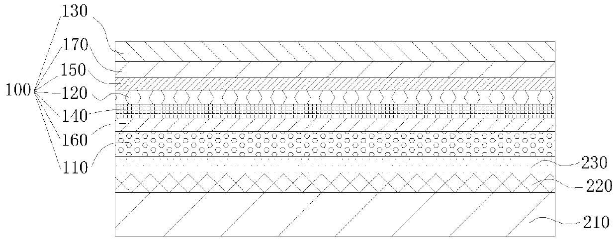
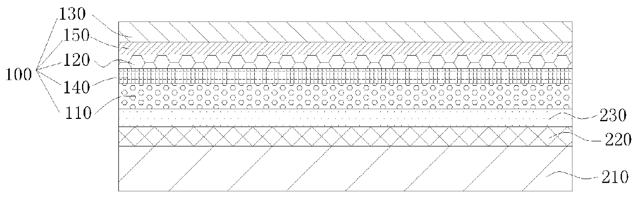
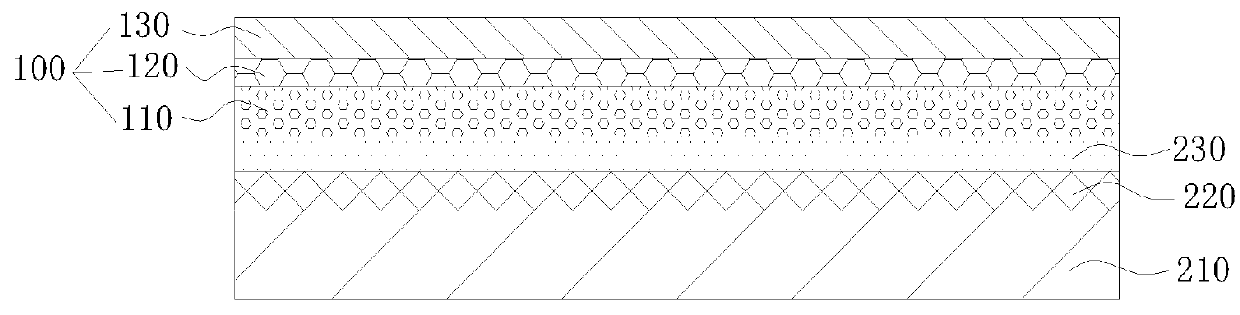
[0026]A clear and complete description will be given to technical solutions of embodiments of the present invention with reference to the attached drawings of the embodiments of the present invention. However, the embodiments so described are only some, but not all, of the embodiments of the present invention. Other embodiments that are available to those having ordinary skills of the art without the expense of creative effort and endeavor are considered belonging to the scope of protection of the present invention.

[0027]Further, the following descriptions of the various embodiments are made with reference to the attached drawings for illustrating, in an exemplary way, specific embodiments to which the present invention is applicable. Directional terminology, such as “up”, “down”, “front”, “rear”, “left”, “right”, “internal”, “external”, and “side”, used in the present invention are described according to the direction shown in the drawings and are not intended to indicate or sugges...


PUM


Abstract

Disclosed is a light-emitting device including a base plate, an orientation layer, a photoluminescence layer, and an electroluminescence assembly. The orientation layer is arranged on the base plate. The photoluminescence layer and the orientation layer are adjacent to and stacked on one another. The orientation layer provides an effect of orientating to the photoluminescence layer. The electroluminescence assembly is arranged on one side of the photoluminescence layer that is distant from the orientation layer or on one side of the base plate that is distant from the orientation layer. The electroluminescence assembly includes a transparent anode, an electroluminescence layer, and a cathode sequentially stacked on each other and the transparent anode faces toward the base plate. Also disclosed are a backlight module including the light-emitting device and a display device including the backlight module.

Description

CROSS REFERENCE TO RELATED APPLICATIONS[0001]This application claims the priority of Chinese Patent Application No. 201610147109.7, entitled “Light-Emitting Device, Backlight Module, and Display Device”, filed on Mar. 15, 2016, the disclosure of which is incorporated herein by reference in its entirety.BACKGROUND OF THE INVENTION1. Field of the Invention[0002]The present invention relates to the field of lighting sources, and in particular to a light-emitting device, a backlight module comprising the light-emitting device, and a display device comprising the backlight module.2. The Related Arts[0003]Light-emitting devices that are commonly known include electroluminescence light-emitting devices and photoluminescence light-emitting devices. The electroluminescence light-emitting devices possess various advantages, such as active luminescence, low power consumption, and light weight, and are thus widely used in all fields. The electroluminescence light-emitting devices are a kind of ...

Claims


Application Information

Patent Timeline
Patent Type & Authority Applications(United States)
IPC IPC(8): H01L51/50H01L51/52
CPCH01L51/5012H01L51/5056H01L51/5092H01L51/5072H01L51/52H10K77/10H10K50/85Y02E10/549H10K59/38H10K50/80H10K50/11H10K50/171H10K50/15H10K50/16H10K99/00
Inventor ZHOU, KAIFENG
Owner SHENZHEN CHINA STAR OPTOELECTRONICS TECH CO LTD
Why Eureka
Try Eureka