Array Imaging Module and Molded Photosensitive Assembly, Circuit Board Assembly and Manufacturing Methods Thereof for Electronic Device
- Summary
- Abstract
- Description
- Claims
- Application Information
AI Technical Summary
Benefits of technology
Problems solved by technology
Method used
Image

Examples
third embodiment
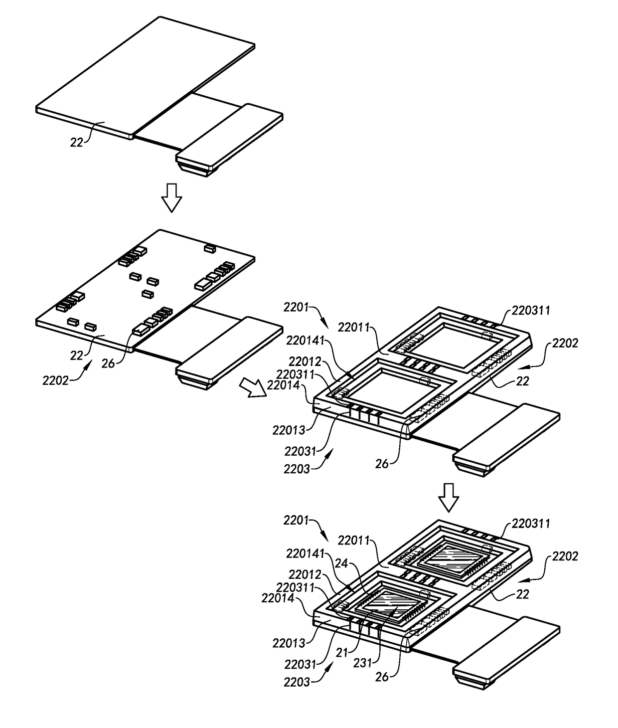
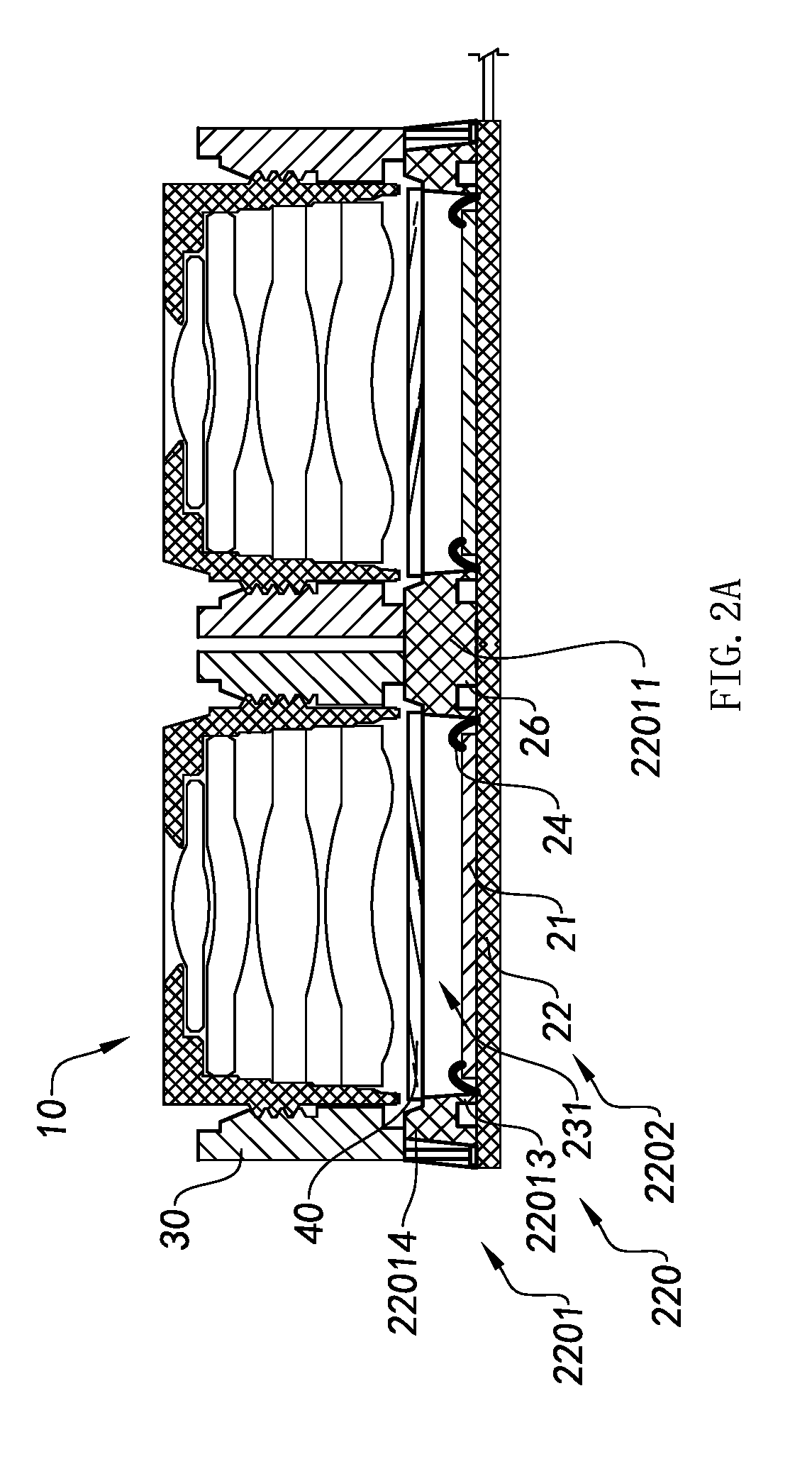
[0245]As shown in FIG. 8, an array imaging module and its circuit board assembly 220 according to the present invention is illustrated.
[0246]Unlike the above embodiment, the circuit board assembly 220 comprises a circuit board 22B, wherein the circuit board 22B has two conductive channels 225B spacedly formed at a bottom side of the photosensitive unit 21 to electrically connect to the circuit board 22B at two lateral sides thereof. The photosensitive unit 21 is coupled at a rear side of the circuit board 22B, wherein the photosensitive area of the photosensitive unit 21 faces upward to receive the light emitting through the optical lens 10.
[0247]In addition, the circuit board 22B comprises two outer indention grooves 226B corresponding to the conductive channels 225B respectively, wherein the two indention grooves 226B serve as a positioning guider for the photosensitive unit 21. In particular, when the photosensitive unit 21 is coupled at the outer indention grooves 226B, the oute...
fourth embodiment
[0251]As shown in FIG. 9, an array imaging module and its circuit board assembly 220 according to the present invention is illustrated.
[0252]The circuit board assembly 220 comprises a reinforcing layer 2204C overlapped and connected to the circuit board 22 to reinforce the strength of the circuit board 22. In other words, the reinforcing layer 2204C is formed at a bottom side of the circuit board 22 corresponding to the area where the photosensitive unit 21 is located. Therefore, the circuit board 22 can be rigidly support the mold sealer 2201 and the photosensitive unit 21.
[0253]In addition, the reinforcing layer 2204C can be metal layer overlapped and connected to the bottom side of the circuit board 22 to enhance the rigidity of the circuit board 22. The reinforcing layer 2204C also has heat dissipating ability that the reinforcing layer 2204C can effectively dissipate heat generated from the photosensitive unit 21.
[0254]It is worth mentioning that the circuit board 22 can be a F...
fifth embodiment
[0255]As shown in FIG. 10, an array imaging module and its circuit board assembly 220 according to the present invention is illustrated.
[0256]Unlike the above embodiments, the circuit board 22D has a least a reinforcing slot 227D, wherein the mold sealer 2201 is extended into the reinforcing slot 227D to enhance the strength of the circuit board 22D.
[0257]The positions of each of the reinforcing slots 227D can be selectively modified according to the rigidity of the circuit board 22D. Preferably, the reinforcing slots 227D are symmetrically formed on the circuit board 22D. Accordingly, the rigidity of the circuit board 22D can be enhanced by the reinforcing slot 227D to reduce the thickness of the circuit board 22D, so as to reduce the thickness of the array imaging module and to enhance the heat dissipation of the circuit board assembly 220.
[0258]It is worth mentioning that the reinforcing slot 227D is embodied as an indention cavity, wherein the reinforcing slot 227D is not a thro...
PUM
 Abstract
Description
Claims
Application Information
 - R&D
- Intellectual Property
- Life Sciences
- Materials
- Tech Scout
- Unparalleled Data Quality
- Higher Quality Content
- 60% Fewer Hallucinations
Browse by: Latest US Patents, China's latest patents, Technical Efficacy Thesaurus, Application Domain, Technology Topic, Popular Technical Reports.
© 2025 PatSnap. All rights reserved.Legal|Privacy policy|Modern Slavery Act Transparency Statement|Sitemap|About US| Contact US: help@patsnap.com