Laminate structure, piezoelectric element, and method of manufacturing piezoelectric element
- Summary
- Abstract
- Description
- Claims
- Application Information
AI Technical Summary
Benefits of technology
Problems solved by technology
Method used
Image

Examples
examples
[0145]Examples and Comparative Examples of the present invention will be described.
example 1
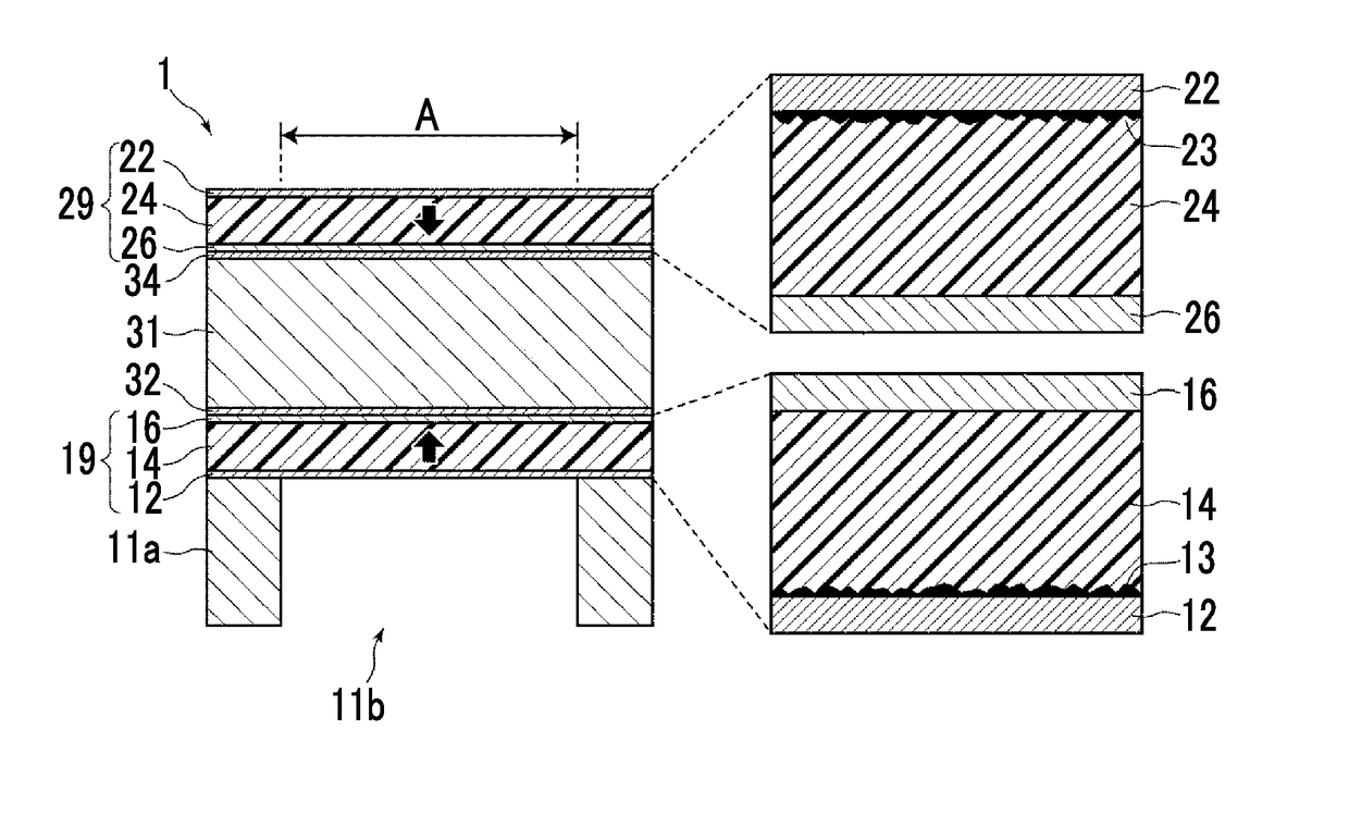
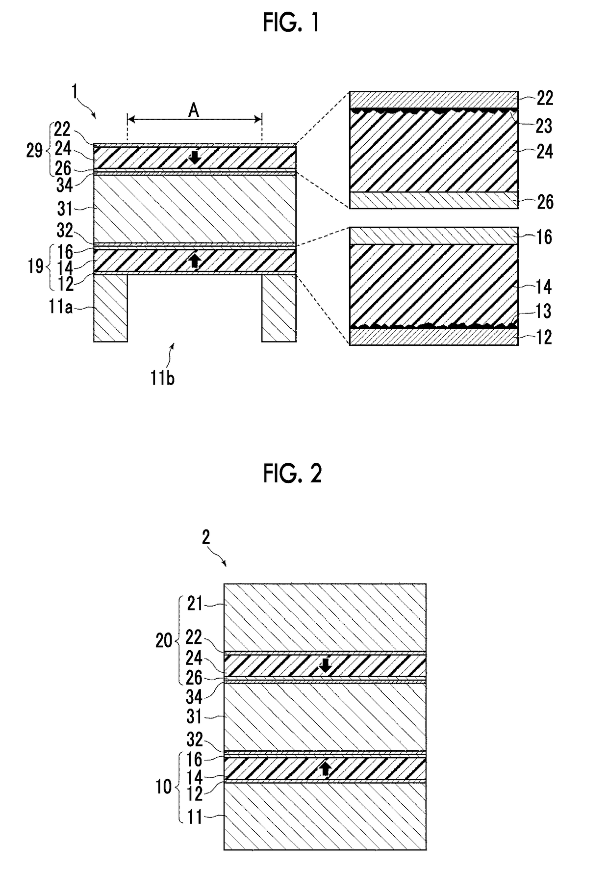
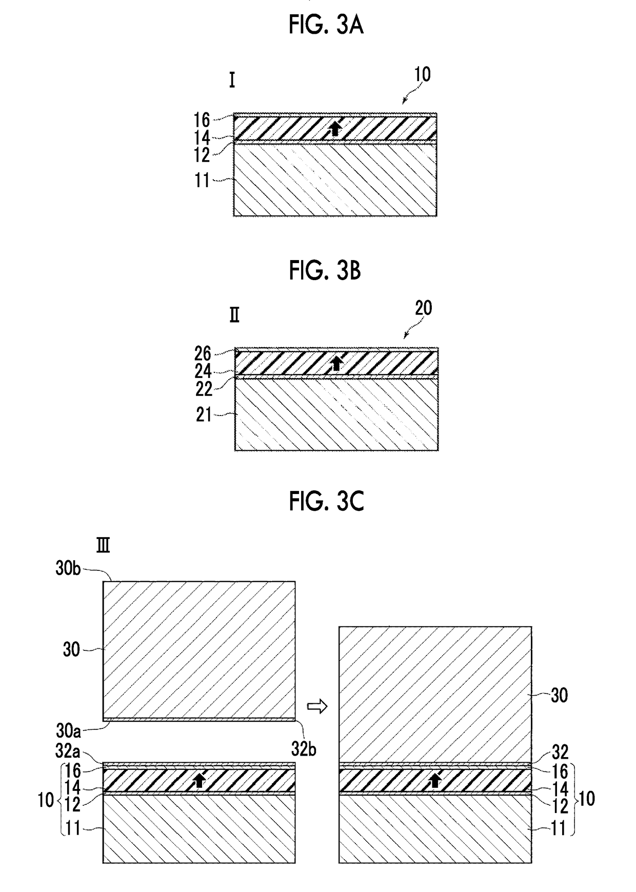
[0146]An Nb-PZT film having a thickness of 3 μm as the first piezoelectric film 14 was formed on a silicon wafer having a thickness of 200 μm and having opposite surfaces polished as the first silicon substrate 11 with an Ir electrode layer as the first electrode layer 12 interposed therebetween. An Ir electrode layer as the first facing electrode layer 16 was further formed on the Nb-PZT film. As a result, the first structure 10 was obtained.
[0147]Likewise, an Nb-PZT film having a thickness of 3 μm as the second piezoelectric film 24 was formed on a silicon wafer having a thickness of 200 μm as the second silicon substrate 21 with an Ir electrode layer as the second electrode layer 22 interposed therebetween. An Ir electrode layer as the second facing electrode layer 26 was further formed on the Nb-PZT film. As a result, the second structure 20 was obtained.
[0148]Each of the Ir electrode layers was obtained to have a thickness of 150 nm using a sputtering method. During the formati...
example 2
[0156]A laminate structure was obtained using the same method as in Example 1, except that the thickness of the second piezoelectric film 24 in the second structure 20 was 1 μm. In the laminate structure according to Example 2, in a case where the first structure 10 side including the first piezoelectric film 14 having a thickness of 3 μm was set as the upper side, a 300 μm protrusion protruded downward from the 6-inch wafer as a whole. Here, the protruding of the 300 μm protrusion represents that, in a case where opposite end portions of the wafer are set as a reference position, the distance from the reference position to the center of the wafer, which is the most protruding portion, in the thickness direction of the wafer, that is, the height difference is 300 μm.
[0157]Next, a cantilever type device was prepared using the same method as in Example 1.
PUM
 Abstract
Description
Claims
Application Information
 - Generate Ideas
- Intellectual Property
- Life Sciences
- Materials
- Tech Scout
- Unparalleled Data Quality
- Higher Quality Content
- 60% Fewer Hallucinations
Browse by: Latest US Patents, China's latest patents, Technical Efficacy Thesaurus, Application Domain, Technology Topic, Popular Technical Reports.
© 2025 PatSnap. All rights reserved.Legal|Privacy policy|Modern Slavery Act Transparency Statement|Sitemap|About US| Contact US: help@patsnap.com