Method of bonding substrates, microchip and method of manufacturing the same

Pending Publication Date: 2018-05-24
USHIO DENKI KK
3 Cites 0 Cited by

AI-Extracted Technical Summary

Problems solved by technology

However, those methods may entail the following problems.
That is to say, in the method of joining by use of the adhesive agent, it is likely that the adhesive agent may seep into a microchannel to occlude the flow channel, a part of the microchannel may become narrower to cause the diameter of the flow channel to be uneven, and further an undesired turbulence may occur in the characteristic, which should be...

Method used

[0093]The substrates 11 and 15 may be made of the same type of material, such as the acrylic resin and the acrylic resin or the COP and the COP, or alternatively made of a material in which different types of resin are combined, such as the COP and the PS. When combining the different resin, it is preferable to make the substrate 11, in which the segmenting recessed portion is fabricated, from a soft or flexible material in hardness, because the segmenting recessed portion acquires a higher flexibility so that the substrate is more likely to tightly adhere.
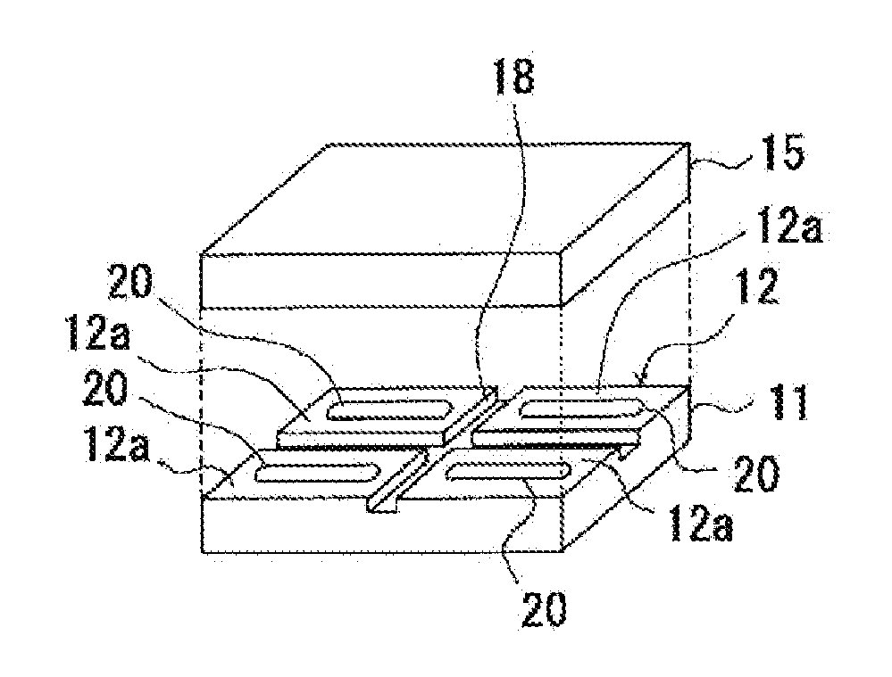
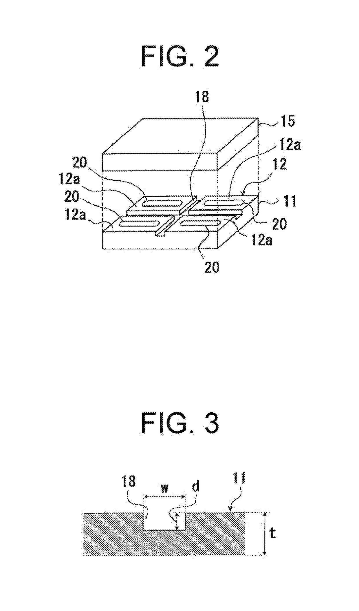
[0107]Also, the segmenting groove 18 are arranged to be across the substrate (or base material) from one end of the substrate to the other end of the substrate so as to provide the higher flexibility to the substrate.
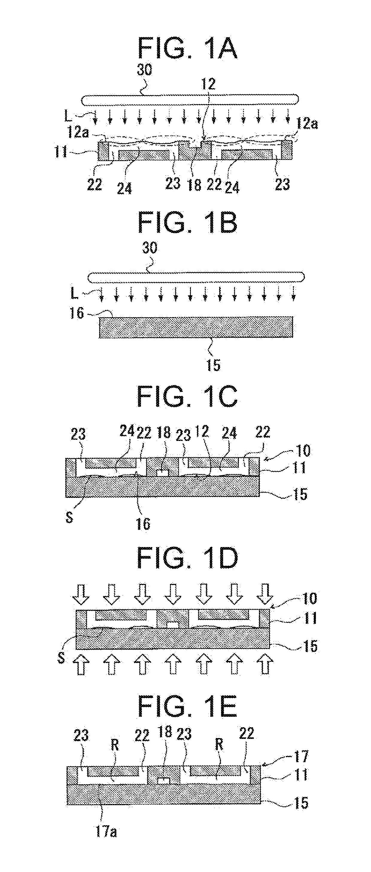
[0142]As described above, as shown in FIG. 1E, it comes to the status in which whole surfaces of the joining surface 12 on the first substrate 11 uniformly contact the joining surface 16 of the second substrate 15. As a result, it makes it possible to avoid any defects, for example, that the defective in joining between the substrates 11 and 15 occurs, that the structural recess 20 serving as the microchannel formed in the substrate 11 is deformed, and that the gas bubbles are caught in the joining boundary 17a between two substrates 11 and 15. Resultantly, it makes it possible to achieve a sufficiently tight adhered state between the first substrate 11 and the second substrate 15 without those defects interfering with the structural recess 20 of the first substrate 11.
[0144]According to the above described method of bonding the substrates, the joining surface 12 of the first substrate 11 is constituted with a plurality of joining regions 12a segmented to be separate from one another by the segmenting groove 18. The area of individual joining region 12a is smaller as compared to the case in which the whole surface of the substrate 11 is constituted ...

Benefits of technology

[0050]According to the above mentioned aspects of the method of bonding the substrates of the various embodiments, the joining surface of the first substrate and/or the joining surface of the second substrate are constituted with a plurality of joining regions segmented to be separate from one another by a segmenting recessed portion. As an area of an individual joining region is sufficiently smaller as compared to the case in which a whole surface of the substrate constitutes one joining surface, it makes it possible to suppress a warpage of the substrate or a roll on the joining surface thereof from adversely affecting. Thus, when the substrates are pressurized in the pressurizing step, in each of the joining regions, a whole surface thereof is capable of being adhered tightly in an assured manner.
[0051]As a result, it makes it possible to make the whole surfaces of the joining boundary in the joined body are tightly adhered to each other in an assured manner. Resultantly, it makes it possible to join the first substrate to the second substrate in a higher adhered state even when at least one of the ...

Abstract

Disclosed herein is a method of bonding substrates, a microchip, and a method of manufacturing the microchip capable of joining two substrates in a higher adhered state even when at least one of the substrate has a warpage or a roll. A method of bonding a first substrate and a second substrate each of which is made of glass or a resin comprises: a surface activating step for activating each of joining surfaces of the first substrate and the second substrate; and a pressurizing step for pressurizing the first substrate and the second substrate in a state that the first substrate and the second substrate are stacked such that respective joining surfaces contact each other. The joining surface of the first substrate and/or the joining surface of the second substrate are constituted with a plurality of joining regions segmented to be separate from one another by a segmenting recessed portion.

Application Domain

Precision positioning equipmentAdhesive processes with surface pretreatment +7

Technology Topic

Electrical and Electronics engineering

Image

  • Method of bonding substrates, microchip and method of manufacturing the same
  • Method of bonding substrates, microchip and method of manufacturing the same
  • Method of bonding substrates, microchip and method of manufacturing the same

Examples

  • Experimental program(6)

Example

Working Examples
[0172]Hereinafter, working examples of the method of bonding substrates according to the present embodiment will be described in detail below. Nevertheless, it should be noted that the present invention is not limited to the following working examples.

Example

Working Example 1
[0173]The first substrate and the second substrate were prepared as follows.
[0174]FIG. 7 is a view illustrating the first substrate prepared according to the working example 1. A first substrate 41A has a profile conforming to the SBS standard (i.e., 85 mm×128 mm). On one face of a plate having the thickness of 2 mm and made of the cycloolefin resin (“ZEONEX 460R” manufactured by ZEON Corporation), a peripheral recessed portion 49A and a segmenting groove 48A are formed by the injection molding. The peripheral recessed portion 49A and the segmenting groove 48A are formed such that six rectangular joining regions 42aA, each having a profile of 36 mm×36 mm, are residually arranged as convex portions in two lines and three columns in parallel longitudinally and transversely.
[0175]The segmenting groove 48A has the width of 2 mm and the depth (that is, the distance from the joining regions 42aA to the innermost portion of the segmenting groove 48A) of 1 mm. Likewise, the peripheral recessed portion 49A also has the depth (that is, the distance from the joining regions 42aA to the innermost portion of the peripheral recess 49A) of 1 mm.
[0176]A second substrate has a profile conforming to the SBS standard (i.e., 85 mm×128 mm). The second substrate is a microplate with 12×8 holes on which structural recesses are formed on a joining face of a plate having the thickness of 2 mm and made of the cycloolefin resin (“ZEONEX 460R” manufactured by ZEON Corporation). A plurality of holes of the microplate, which serve as the structural recesses, respectively, are independent of one another. In this regard, although it does not have a so-called microchip structure in which two holes are coupled to each other through a flow channel, it is assumed that each of the holes of the microplate is to be the injection port and the discharge port of the microchip so as to perform the bonding. It is also assumed that the hole to be serve as the structural recess of the respective holes of the microplate is opposed to the same joining region 42aA on the opposing first substrate. In FIG. 7, the chained line denotes the positon of the hole in the second substrate corresponding to the first substrate 41A.
[0177]The above prepared first substrate 41A and the second substrate were bonded to each other by performing the following ultra violet light irradiation step and the joining step.
(Ultra Violet Light Irradiation Step)
[0178]Using a xenon excimer lamp, respective joining surfaces of the two substrates were irradiated with the vacuum ultra violet light under the condition of the illuminance of 40 mW/cm2 and the irradiation time of 20 seconds.
(Joining Step)
[0179]The two substrates were stacked such that respective joining surfaces thereof contact each other so as to obtain a stacked body (Stacking Step). Subsequently, the stacked body were pressurized under the condition of the pressure of 0.2 MPa, the pressurizing time of 300 seconds, and the heating temperature of 90 degrees Celsius so as to join the two substrates, and resultantly a joined body [A] was obtained.

Example

Working Example 2
[0180]Two substrates were joined and the joined body [B] were obtained similarly to the working example 1, except that the first substrate was prepared as follows.
[0181]FIG. 8 is a view illustrating the first substrate prepared according to the working example 2. A first substrate 41B has a profile conforming to the SBS standard (i.e., 85 mm×128 mm). On one face of a plate having the thickness of 2 mm and made of the cycloolefin resin (“ZEONEX 460R” manufactured by ZEON Corporation), a peripheral recessed portion 49B and a segmenting groove 48B are formed by the injection molding. The peripheral recessed portion 49B and the segmenting groove 48B are formed such that twelve elongated rectangular joining regions 42aB, each having a profile of 18 mm×36 mm, are residually arranged as convex portions in two lines and six columns in parallel longitudinally and transversely.
[0182]The segmenting groove 48B has the width of 2 mm and the depth (that is, the distance from the joining regions 42aB to the innermost portion of the segmenting groove 48B) of 1 mm. Likewise, the peripheral recessed portion 49B also has the depth (that is, the distance from the joining regions 42aB to the innermost portion of the peripheral recessed portion 49B) of 1 mm.

PUM

PropertyMeasurementUnit
Thickness5.0E-5m
Pressure
Width

Description & Claims & Application Information

We can also present the details of the Description, Claims and Application information to help users get a comprehensive understanding of the technical details of the patent, such as background art, summary of invention, brief description of drawings, description of embodiments, and other original content. On the other hand, users can also determine the specific scope of protection of the technology through the list of claims; as well as understand the changes in the life cycle of the technology with the presentation of the patent timeline. Login to view more.

Similar technology patents

Light guide plate and a planar lighting device using the same

InactiveUS20070147759A1suppress warpageuneven brightness be reduce
Owner:FUJIFILM CORP

Liquid resin composition for compression molding and electronic component apparatus

PendingUS20200181392A1suppress warpage
Owner:NAMICS CORPORATION +1

Multilayer ceramic capacitor

ActiveUS20150340156A1dielectric thickness be reducehigh reliability
Owner:MURATA MFG CO LTD

Glass sheet

InactiveUS20180009707A1suppress warpage
Owner:ASAHI GLASS CO LTD

Optical fiber sensor

InactiveUS20090034901A1high reliabilitymoderate intensity
Owner:MITSUBISHI ELECTRIC CORP

Classification and recommendation of technical efficacy words

  • suppress warpage
  • high reliability

Light guide plate and a planar lighting device using the same

InactiveUS20070147759A1suppress warpageuneven brightness be reduce
Owner:FUJIFILM CORP

Liquid resin composition for compression molding and electronic component apparatus

PendingUS20200181392A1suppress warpage
Owner:NAMICS CORPORATION +1

Glass sheet

InactiveUS20180009707A1suppress warpage
Owner:ASAHI GLASS CO LTD
Why Eureka
Try Eureka