Semiconductor device

Active Publication Date: 2018-05-24
MURATA MFG CO LTD
View PDF4 Cites 1 Cited by
  • Summary
  • Abstract
  • Description
  • Claims
  • Application Information

AI Technical Summary

Benefits of technology

The present disclosure aims to provide a semiconductor device that can improve wire connection and increase its reliability. It achieves this by designing a patch portion that raises the bottom of a hollow portion, reducing the depression in the surface of a second metal layer when it is formed. This makes wire bonding more reliable. Additionally, the patch portion has a trapezoidal cross-sectional shape, which prevents the formation of defects in a metal layer or insulation layer when covering the patch portion, increasing its reliability. The angle of the patch portion corner is large, which prevents defects in the metal layer or insulation layer when covering the patch portion, flattening the surface of the electrode pad to reduce poor wire connection.

Problems solved by technology

When wire bonding is performed on such an electrode pad, poor connection may occur due to the depression.
As a result, a problem arises in that decrease of the mechanical strength in connecting between a wire and the electrode pad and increase of the electrical resistance between the wire and the electrode pad may occur.
Therefore, for example, an insulation film that is made of an organic material and has a large thickness is not taken into consideration, and, if an electrode pad is formed so as to fill a deep through-hole, the dummy pattern may not be capable of flattening the electrode pad.
In this case, when a metal layer or an insulation layer is formed so as to cover the dummy pattern, the metal layer or the insulation layer is not likely to be appropriately formed at a corner of the quadrangular cross-sectional shape, and a problem arises in that reliability tends to decrease.

Method used


Image

  • Semiconductor device
  • Semiconductor device
  • Semiconductor device

Examples


first embodiment

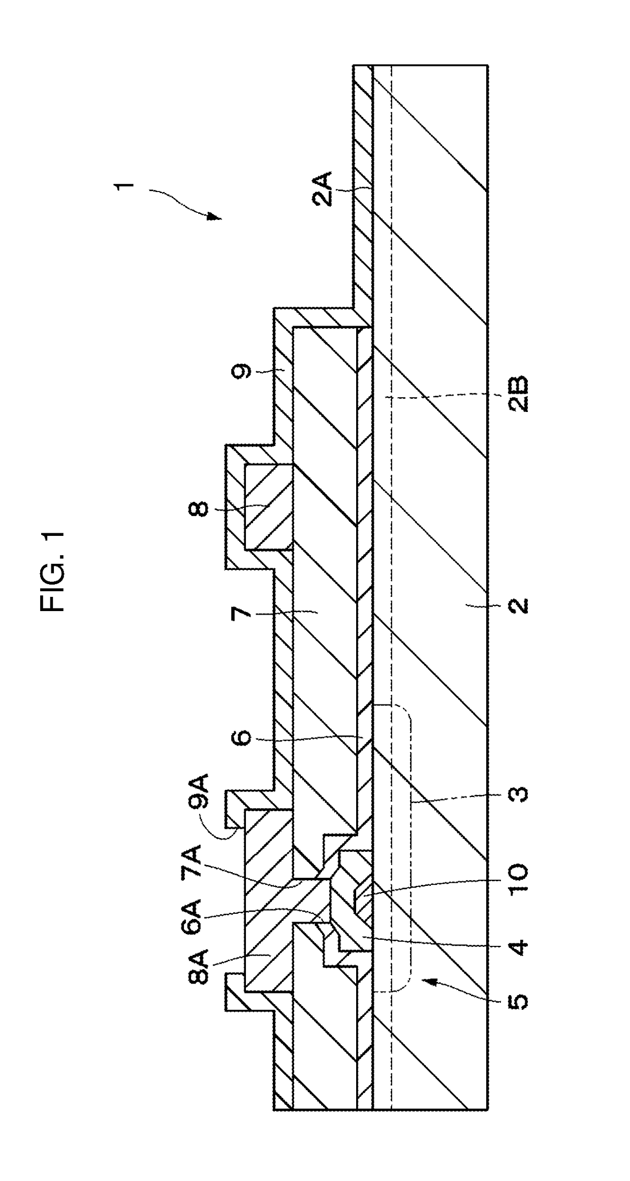
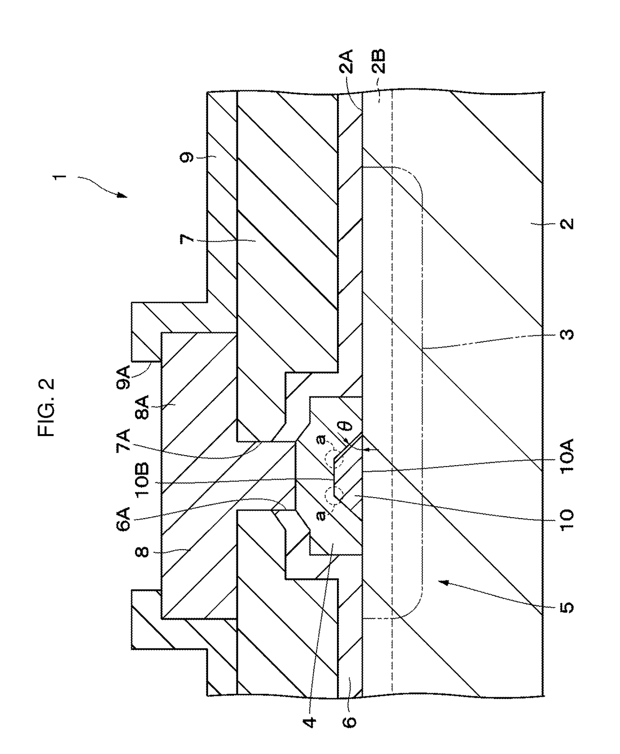
[0021]FIGS. 1 and 2 illustrate a semiconductor device 1 according to a The semiconductor device 1 includes a semiconductor substrate 2, a first metal layer 4, an insulation layer 6, an organic layer 7, a second metal layer 8, and a patch portion 10. The first metal layer 4, the insulation layer 6, the organic layer 7, and the second metal layer 8 are sequentially stacked on a surface 2A of the semiconductor substrate 2.

[0022]The semiconductor substrate 2 is a planar substrate made of a semiconductor material, such as gallium arsenide (GaAs). Alternatively, the semiconductor substrate 2 may be made of another group III-V compound semiconductor, such as indium phosphide (InP) or gallium nitride (GaN). Further alternatively, the semiconductor substrate 2 may be made of a group II-VI compound semiconductor, such as zinc selenide (ZnSe), or a group IV compound semiconductor, such as silicon carbide (SiC) or silicon germanium (SiGe). Instead of a compound semiconductor, the semiconductor...

second embodiment

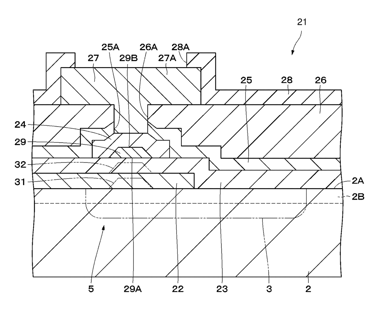
[0053]In the second embodiment, the patch portion 29 is disposed at the interface between the insulation layer 23 and the first metal layer 24. This is not a limitation on the present disclosure. The patch portion 29 may be disposed at any position in a region between the surface 2A of the semiconductor substrate 2 and the via 26A of the organic layer 26 in the thickness direction. Therefore, as shown by a two-dot chain line in FIG. 3, a patch portion 31 may be disposed at the interface between the semiconductor substrate 2 and the first metal layer 22, or a patch portion 32 may be disposed at the interface between the first metal layer 22 and the insulation layer 23.

[0054]In each of the embodiments described above, a single patch portion 10 or 29 is disposed between the surface 2A of the semiconductor substrate 2 and the via 7A or 26A of the organic layers 7 or 26 in the thickness direction. This is not a limitation on the present disclosure. A plurality of patch portions may be di...


PUM


Abstract

A semiconductor device includes a semiconductor substrate, a first metal layer, an insulation layer, an organic layer, and a second metal layer. The first metal layer, the insulation layer, the organic layer, and the second metal layer are sequentially stacked on a surface of the semiconductor substrate. The first metal layer and the second metal layer are electrically connected to each other through vias formed in the insulation layer and the organic layer. The second metal layer includes an electrode pad at a position corresponding to the positions of the vias. At the interface between the surface of the semiconductor substrate and the first metal layer, a patch portion having a trapezoidal cross-sectional shape is disposed directly below the vias.

Description

[0001]This application claims priority from Japanese Patent Application No. 2016-227019 filed on Nov. 22, 2016. The content of this application is incorporated herein by reference in its entirety.BACKGROUND OF THE DISCLOSURE1. Field of the Disclosure[0002]The present disclosure relates to a semiconductor device in which an organic insulation layer is formed on or over a semiconductor substrate.2. Description of the Related Art[0003]Semiconductor devices in which an insulation layer is formed on or over a surface of a semiconductor substrate are generally known (see, for example, Japanese Unexamined Patent Application Publication No. 7-153756 (Patent Document 1)). The semiconductor device described in Patent Document 1 includes a semiconductor substrate and an interlayer insulation film formed over a surface of the semiconductor substrate. The interlayer insulation film is interposed between a lower wiring layer and an upper wiring layer, and the lower wiring layer and the upper wiri...

Claims


Application Information

Patent Timeline
IPC IPC(8): H01L23/528H01L23/522H01L23/532
CPCH01L23/5283H01L23/5226H01L23/53295H01L24/02H01L24/08H01L24/29H01L2224/04026H01L2224/0805H01L2224/08057H01L2224/29009H01L23/3171H01L24/05H01L2224/04042H01L2224/05016H01L2224/05022H01L2224/05076H01L2224/05082H01L2224/05091H01L2224/05144H01L2224/05559H01L2224/05567H01L2224/05644H01L2224/45099H01L2924/00014
Inventor KOBAYASHI, KAZUYASANO, YUICHITOKUDA, DAISUKETOKUYA, HIROAKI
Owner MURATA MFG CO LTD
Why Eureka
Try Eureka