Check patentability & draft patents in minutes with Patsnap Eureka AI!

Polarized Light Emission From Micro-Pixel Displays and Methods of Fabrication Thereof

a technology of micro-pixel displays and light emission, applied in static indicating devices, instruments, mechanical devices, etc., can solve the problems of efficiency drooping at higher current densities, less energy efficient, and large, and achieve the effect of reducing the number of transistors

Active Publication Date: 2018-06-07
OSTENDO TECH INC
View PDF3 Cites 42 Cited by
  • Summary
  • Abstract
  • Description
  • Claims
  • Application Information

AI Technical Summary

Benefits of technology

The patent text describes a new invention related to solid state light emitters such as LEDs and laser diodes. The invention takes advantage of the unique crystallographic properties of III-nitride materials to create solid state light emitting structures that are more efficient and energy-efficient compared to traditional c-plane growth materials. The non-c-plane growth materials, such as m-plane and semipolar planes, show an unequal photon emission that is dependent on the direction of the electric vector, resulting in higher efficiency and lower energy consumption. The use of non-c-plane growth materials also reduces the efficiency droop that occurs at higher current densities. The invention is based on the use of non-c-plane growth materials, such as the m-plane, to create more efficient and energy-efficient solid state light emitting structures.

Problems solved by technology

The use of unpolarized light requires that such display systems incorporate multiple polarizers and polarizing optics, making them larger, more complex, less energy efficient, and costly.
Another undesirable consequence of c-plane growth is the efficiency droop that occurs at higher current densities (Y. C. Shen, G. O. Mueller, S. Watanabe, N. F. Gardner, A. Munkholm, and M. R. Krames, “Auger recombination in InGaN measured by photoluminescence,” Applied Physics Letters, 91, 141101 (2007)).
Nonetheless, this remains an additional element to be placed onto the semiconductor chip in order for polarized light emission to occur and the above prior art mentions nothing about how to actually incorporate the polarization technology into a display product.
No prior art has been identified that describes a systematic method for achieving selective polarization states by utilizing various crystallographic planes of semiconductor materials for micro-LED display purposes.

Method used


Image

  • Polarized Light Emission From Micro-Pixel Displays and Methods of Fabrication Thereof
  • Polarized Light Emission From Micro-Pixel Displays and Methods of Fabrication Thereof
  • Polarized Light Emission From Micro-Pixel Displays and Methods of Fabrication Thereof

Examples


Embodiment Construction

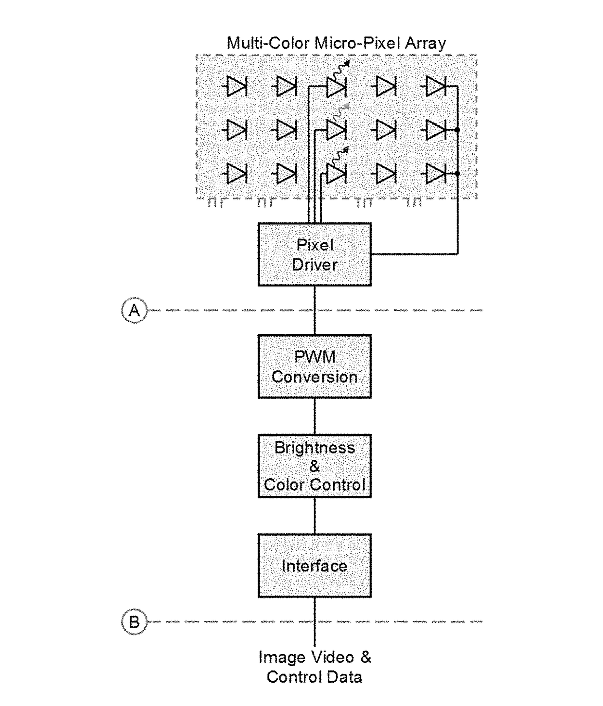
[0025]The above-referenced QPI emissive display device is but one example of an emissive micro-scale pixel array U.S. Pat. Nos. 7,623,560, 7,767,479, 7,829,902, 8,049,231, 8,243,770, 8,098,265, 8,567,960, referred to in the exemplary embodiments described below. However, it is to be understood that the illustrated QPI emissive display device is merely an example of the types of light emitting devices that may be used in and fabricated by the present invention, some of which have been previously set forth. Thus, in the description to follow, references to a QPI emissive display device are to be understood to be for purposes of specificity in the embodiments disclosed, and not for any limitation of the present invention U.S. Pat. No. 7,623,560.

[0026]FIG. 3A and FIG. 3B show the cross-section and light emitting surface of a prior art QPI emissive display device or QPI imager as the c-plane and FIGS. 4A-4C show the side views and light emitting surface as the m-plane in a preferred embo...


PUM


Abstract

A method and apparatus for achieving selective polarization states of emitted visible or other light in a stacked multicolor emissive display device by utilizing nonpolar, semipolar or strained c-plane crystallographic planes of semiconductor materials for light emitting structures within an electronic emissive display device.

Description

CROSS-REFERENCE TO RELATED APPLICATIONS[0001]This application claims the benefit of U.S. Provisional Patent Application No. 62 / 429,033 filed Dec. 1, 2016.BACKGROUND OF THE INVENTION1. Field of the Invention[0002]The invention relates to solid state light emitters such as LEDs and laser diode structures. More specifically, the invention relates to solid state light emitting structures fabricated from III-nitride materials that take advantage of III-nitride material's unique crystallographic properties whereby polarized light is emitted from the light emitting structures.2. Prior Art[0003]Solid state light emitters are at the forefront of today's commercially-available electronic display systems. Many display systems utilize the properties of light polarization in order to obtain increased contrast ratios between “on” and “off” pixels on the display element. The use of unpolarized light requires that such display systems incorporate multiple polarizers and polarizing optics, making th...

Claims


Application Information

Patent Timeline
IPC IPC(8): F21V8/00H01L33/06H01L33/08H01L33/16H01L33/32H01L33/38H01L33/58H01L27/15G09G3/32G09G3/20
CPCG02B6/0056H01L33/06H01L33/08H01L33/16H01L33/32H01L33/387G09G2320/064H01L27/156G02B6/0078G09G3/32G09G3/2003G09G2300/046G09G3/36H01L33/58G09G2310/0264H01L25/0756H01L33/382
Inventor EL-GHOROURY, HUSSEIN S.DEMILLE, NATALIE
Owner OSTENDO TECH INC
Features
  • R&D
  • Intellectual Property
  • Life Sciences
  • Materials
  • Tech Scout
  • Unparalleled Data Quality
  • Higher Quality Content
  • 60% Fewer Hallucinations
Learn More