Eureka AIR delivers breakthrough ideas for toughest innovation challenges, trusted by R&D personnel around the world.

Driver circuit and semiconductor module having same

a driver circuit and semiconductor technology, applied in the direction of transistors, electronic switching, pulse techniques, etc., can solve the problems of high impedance between the source of the main switch and the low-voltage side power supply terminal of the driver circuit, and the main switch is more prone to erroneous switching on or off, so as to suppress the rapid change of current (di/dt), increase the resistance of a current limiting resistor, and prevent extremely large currents

Active Publication Date: 2018-06-07
FUJI ELECTRIC CO LTD
View PDF4 Cites 12 Cited by
  • Summary
  • Abstract
  • Description
  • Claims
  • Application Information

AI Technical Summary

Benefits of technology

The present invention provides a driver circuit that prevents rapid changes in current and excessive current flow when a power semiconductor device switches on or off. This is achieved by using a current limiting resistor to reduce the current flow from the reference voltage of the driver circuit to the source of the main switch when the source takes a negative voltage. This circuit design helps to suppress the flow of current from the low-side power supply of the driver circuit and minimize the impact of switching events on the overall circuit performance.

Problems solved by technology

(1) When the resistance of the current limiting resistor (RR) is set to a large value, the impedance between the source of the main switch and the low-voltage side power supply terminal of the driver circuit becomes high regardless of whether the main switch is ON or OFF. As a result, the main switch is more prone to erroneously switching ON or OFF due to other switches (not illustrated in the figure) in the driver circuit switching ON and OFF or due to external noise.

Method used


Image

  • Driver circuit and semiconductor module having same
  • Driver circuit and semiconductor module having same
  • Driver circuit and semiconductor module having same

Examples


Embodiment Construction

[0035]Next, an embodiment of the present invention will be described in detail.

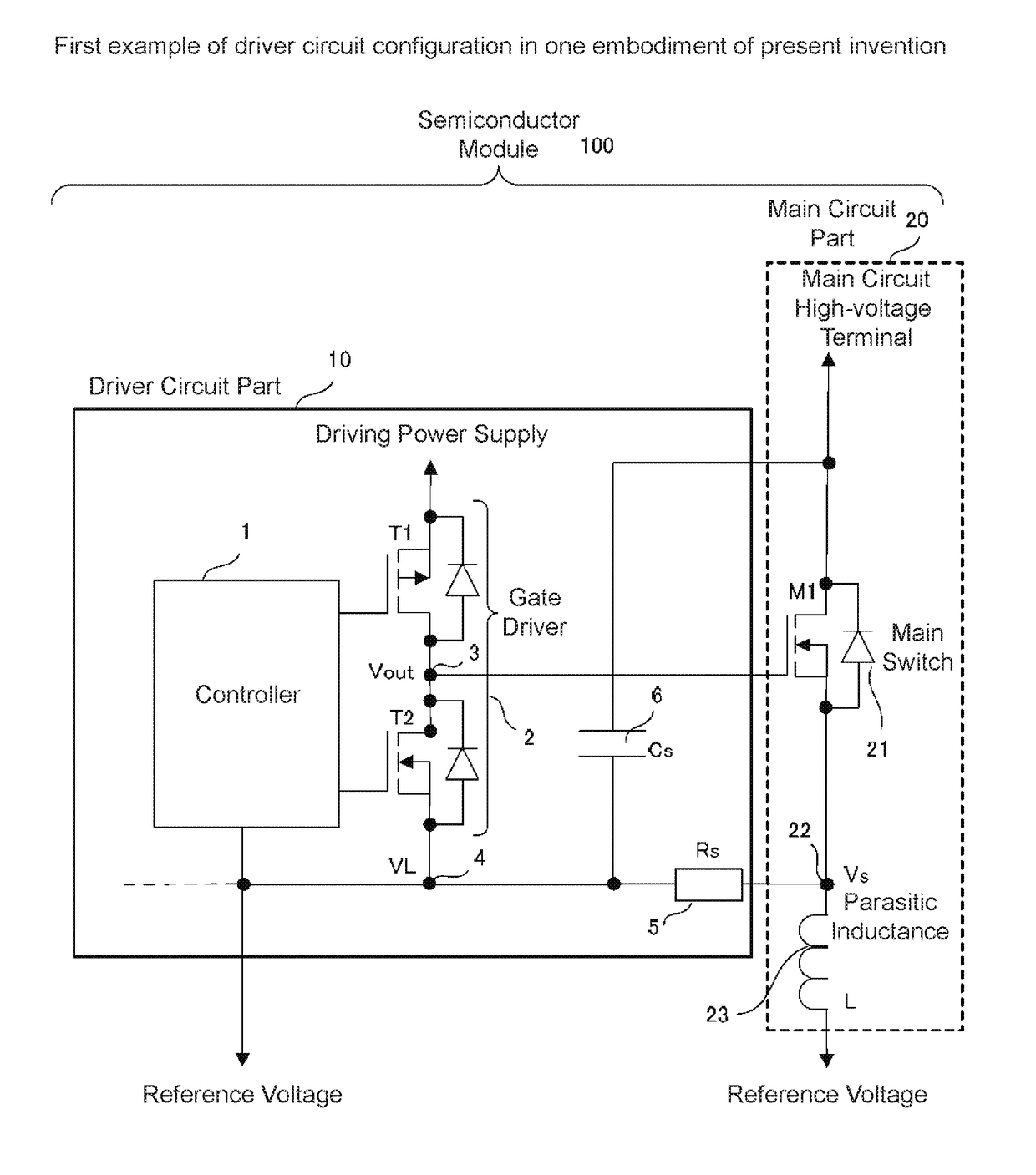
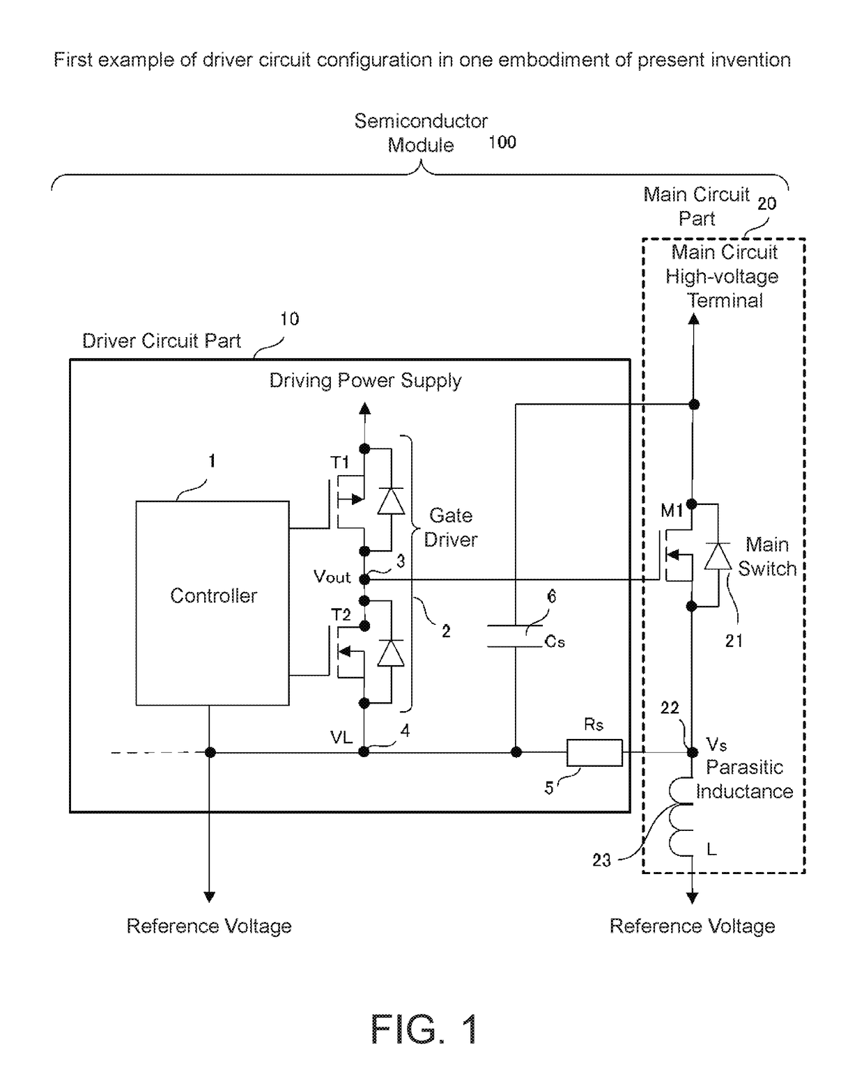
[0036]FIG. 1 illustrates a configuration of a driver circuit according to the embodiment of the present invention. The driver circuit according to the embodiment of the present invention can be generally divided into a driver circuit 10 and a main circuit 20. In this case, the driver circuit 10 and the main circuit 20 can be embedded in a single product to form a semiconductor module 100.

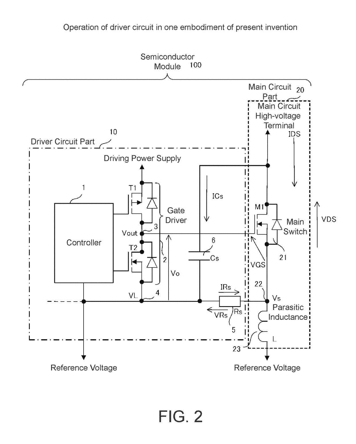
[0037]The driver circuit 10 illustrated in FIG. 1 includes a controller 1 that controls and drives a gate driver 2; the gate driver 2, in which a first transistor T1 and a second transistor T2 are directly connected in series between a driving power supply and a reference voltage, and in which an output (Vout) 3 is obtained from a node between the transistors T1 and T2; a current limiting resistor (RS) 5 connected between a low-voltage side power supply terminal (VL) 4 of the gate driver 2 (the source of the second transi...


PUM


Abstract

An output of a gate driver that drives a main switch is connected to the gate of the main switch, and a low-voltage side power supply terminal of the gate driver is connected to a source of the main switch via a current limiting resistor. Moreover, a suppression capacitor for suppressing rapid changes in current, having a prescribed capacitance, is connected between the drain of the main switch of a main circuit and the low-voltage side power supply terminal of the gate driver. This makes it possible to suppress the rapid change in current that occurs when the main switch switches OFF as well as to prevent extremely large currents from occurring in a low-voltage side power supply line of the driver circuit.

Description

BACKGROUND OF THE INVENTION[0001]Technical Field[0002]The present invention relates to a driver circuit for use in a power converter such as a DC-DC converter or an inverter for driving a motor, and to a semiconductor module including the driver circuit.Background Art[0003]In discrete power semiconductors such as metal-oxide-semiconductor field-effect transistors (MOSFETs) and insulated-gate bipolar transistors (IGBTs), as well as in intelligent power modules (IPMs) and modules that include such devices in a single product, driver circuits are used to drive the power semiconductor devices (hereinafter, main switches). In the driver circuit illustrated in FIG. 5, for example, an output terminal (Vout) 73 of a gate driver 72 in a driver circuit 70 is connected to the gate of a main switch (M11) 81 of a main circuit 80, another terminal (a low-side power supply terminal (VL) 74 of the driver circuit 70) is connected to a source (VS) 82 of a power semiconductor device (the main switch M...

Claims


Application Information

Patent Timeline
Patent Type & Authority Applications(United States)
IPC IPC(8): H03K17/081
CPCH03K17/08104H03K2217/0063H03K2217/0072H03K17/08122H03K17/6871H02M1/32H02M3/158H02M1/0038
Inventor SATO, TADAHIKO
Owner FUJI ELECTRIC CO LTD
Why Eureka
Eureka Blog
Learn More