Ceramic electronic component and manufacturing method thereof

Inactive Publication Date: 2018-06-14
MURATA MFG CO LTD
View PDF2 Cites 1 Cited by
  • Summary
  • Abstract
  • Description
  • Claims
  • Application Information

AI Technical Summary

Benefits of technology

[0019]The step of forming the modified layer may be performed by laser irradiation, electron beam irradiation, or local heating by an image furnace. In these methods, only a specific site of the ceramic body can be locally heated without using a mask or the like prepared in advance, and therefore, the productivity is very high. Since local heating heats and modifies only the surface layer portion of the ceramic body, there is no substantial effect on the electrical characteristics as the electronic component. In particular, laser irradiation is advantageous in that the apparatus can be constructed relatively small, and the irradiation position of laser can be quickly changed. A known laser such as YAG laser or YVO4 laser can be used for the laser.
[0020]As a method of plating treatment in the present disclosure, either electroplating or electroless plating can be used. In the case of electroplating, there is an advantage that it is easy to control the film thickness.
[0021]One of the features of the method of the present disclosure is that electrodes can be easily formed at any sites. For example, when modified layers are formed only on both longitudinal end surfaces of a ceramic body and on one surface (for example, the bottom surface) ad

Problems solved by technology

In these techniques, there is a problem that the thickness of the electrode is increased due to the application of the electrode paste, and the external dimension is increased correspondingly.
In this method, however, as the core for depositing the plating, it is necessary to expose the ends of the plurality of internal electrodes and the anchor tab

Method used


Image

  • Ceramic electronic component and manufacturing method thereof
  • Ceramic electronic component and manufacturing method thereof
  • Ceramic electronic component and manufacturing method thereof

Examples


first embodiment

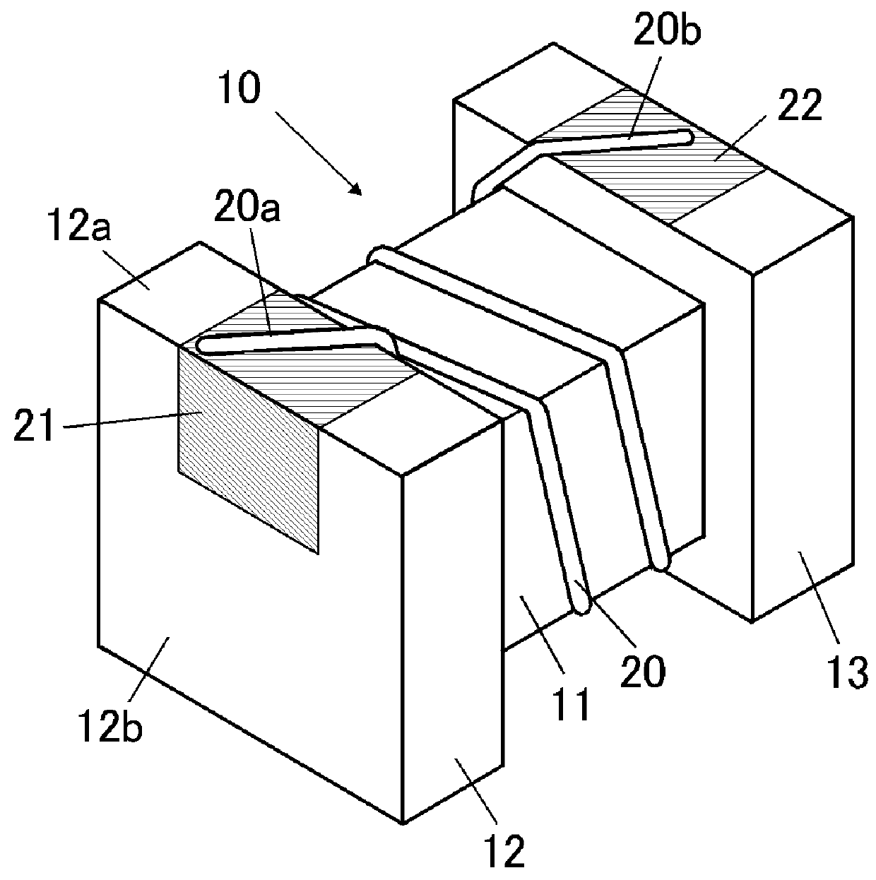
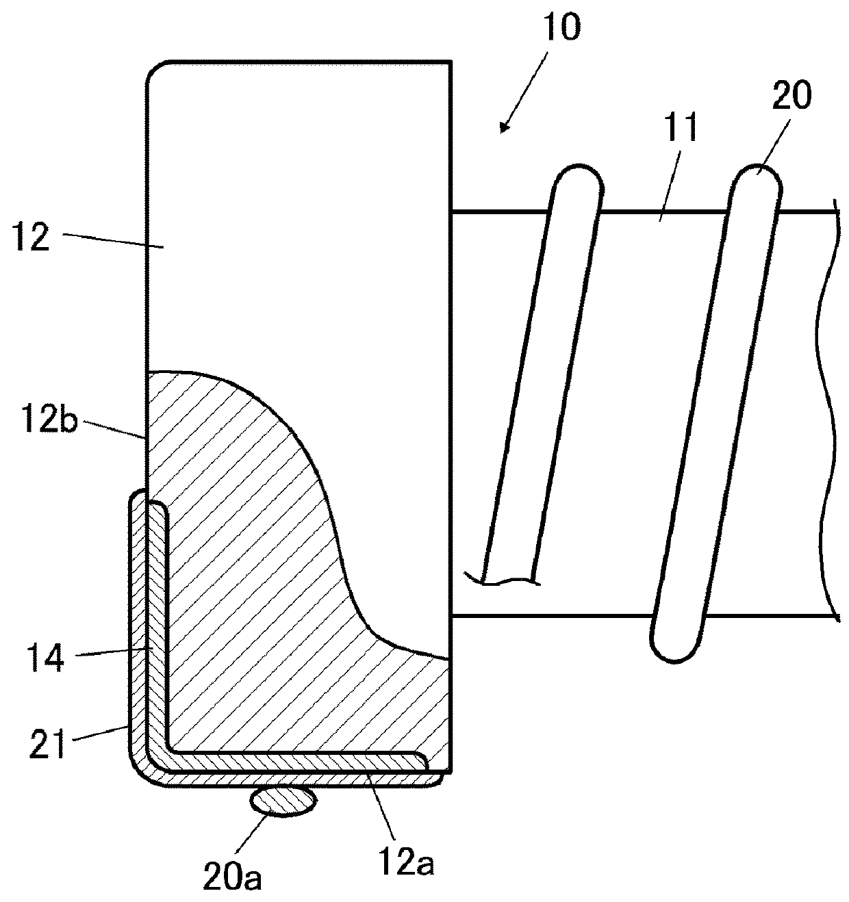
[0041]FIG. 1 shows a wire-wound inductor 1 as the ceramic electronic component according to the present disclosure. In FIG. 1, the bottom surface of the inductor 1 is shown to face upward. The inductor 1 includes a winding core portion 11, a core (ceramic body) 10 having flange portions 12 and 13 formed at both ends of the winding core portion 11, a wire 20 wound around the winding core portion 11, and external electrodes 21 and 22 to which both ends 20a and 20b of the wire 20 are electrically connected. It should be noted that the drawings including FIG. 1 are all schematic, and their dimensions, scales of aspect ratios, etc. may differ from actual products.

[0042]The core 10 is made of, for example, a sintered ceramic material containing a metal oxide, such as a Ni—Cu—Zn ferrite, a Ni—Zn ferrite or a Mn—Zn ferrite. FIG. 2 is an enlarged sectional view of a portion of the wire-wound inductor 1 shown in FIG. 1, and is a sectional view showing the vicinity of one flange portion 12 of ...

second embodiment

[0068]FIG. 14 shows an example of a common mode choke coil 50 of two lines (four terminals) as the present disclosure. FIG. 14 shows the coil component 50 turned upside down. In this coil component 50, a winding core portion 52 is provided at the center portion of a ferrite core (ceramic body) 51, and a pair of flange parts 53 and 54 is provided at both axial ends. A plurality of wires is wound around the winding core portion 52. For example, two wires (not shown) may be wound in parallel on the winding core portion 52. Two (four in total) external electrodes 55 to 58 are respectively formed from the bottom surfaces to the outer surfaces of the flange parts 53 and 54. One ends of the two wires may be connected and fixed on the external electrodes 55 and 56 of the one end side flange portion 53, and the other ends of the wires may be connected and fixed on the external electrodes 57 and 58 of the other end side flange portion 54.

[0069]In this embodiment, similarly to FIG. 2, a modifi...


PUM


Abstract

A ceramic electronic component and manufacturing method are capable of easily forming a plating electrode on any portion of a surface of a ceramic body. The ceramic electronic component includes a ceramic body containing a metal oxide, a modified layer formed on a surface layer portion of the ceramic body, on which a portion of the metal oxide is melted and solidified, and an electrode comprising a plated metal formed on the modified layer. In the modified layer, at least one of metal elements constituting the metal oxide is segregated. Plated metal is likely to be deposited due to segregation of the metal elements.

Description

CROSS-REFERENCE TO RELATED APPLICATION[0001]This application claims benefit of priority to Japanese Patent Application No. 2016-242002, filed Dec. 14, 2016, the entire content of which is incorporated herein by reference.BACKGROUNDTechnical Field[0002]The present disclosure relates to a ceramic electronic component, and particularly to a ceramic electronic component in which a plating electrode is formed on the surface of a ceramic body and a method for manufacturing the same.Description of the Related Art[0003]Conventionally, as a method of forming an external electrode of an electronic component, it is general to apply an electrode paste to both end surfaces of a ceramic body, subsequently bake or thermally cure the electrode paste to form a base electrode, and then form a plating electrode on the base electrode by plating treatment.[0004]For the application of the electrode paste, a method of immersing an end of the electronic component in a paste film formed with a predetermined...

Claims


Application Information

Patent Timeline
IPC IPC(8): H01F27/24H01F27/29H01F41/02
CPCH01F27/24H01F27/29H01F41/02H01F41/00H01F1/344H01F17/045H01F27/255H01F27/292H01F41/10H01G4/232H01G4/2325H01G4/252H01G4/30
Inventor ISHIDA, TAKUYAMAKI, YOSHIFUMIHIRAI, SHINYA
Owner MURATA MFG CO LTD
Why Eureka
Try Eureka