Inspection apparatus and inspection method using the same

a technology of inspection apparatus and inspection method, which is applied in the direction of semiconductor/solid-state device testing/measurement, instruments, material analysis, etc., can solve the problems of affecting the lifetime of the organic light-emitting display device, affecting and the encapsulation layer formed in the bending area or the scribing line may be damaged, so as to reduce defects and effectively determine the

Active Publication Date: 2018-07-05
LG DISPLAY CO LTD
View PDF12 Cites 10 Cited by
  • Summary
  • Abstract
  • Description
  • Claims
  • Application Information

AI Technical Summary

Benefits of technology

[0020]According to the aspects of the present disclosure, by disposing a polarizer and an analyzer in an inspection apparatus for inspecting a substrate formed of a transparent film, the recognition of the transparent film can be improved, such that it can be effectively determined whether there is the transparent film.
[0021]According to the aspects of the present disclosure, by including a scan camera in the inspection apparatus, scan inspection rather than spot inspection can be carried out, such that the portions where the transparent film should not be deposited can be scanned along the periphery of a plurality of cells, thereby reducing defects.
[0022]According to the aspects of the present disclosure, the inspection equipment includes a light source emitting light having a wavelength of 400 nm to 800 nm, such that the recognitio

Problems solved by technology

Unfortunately, the organic light emitting element can easily deteriorate by internal factors such as deterioration of the electrodes and the emission layer due to oxygen, deterioration by the reaction between the emission layer and interfaces, etc., as well as external factors such as moisture, oxygen, ultraviolet ray and fabricating conditions of the device.
Among these, oxygen and moisture introduced from the outside seriously affect the lifetime of the organic light emitting display device, and thus encapsulation of the device is very important.
The portion of the encapsulation layer formed in the bending area o

Method used


Image

  • Inspection apparatus and inspection method using the same
  • Inspection apparatus and inspection method using the same
  • Inspection apparatus and inspection method using the same

Examples


Embodiment Construction

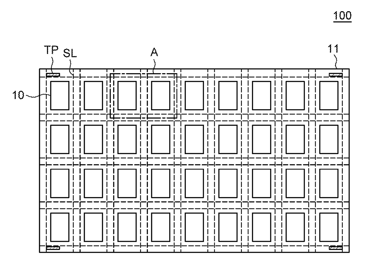
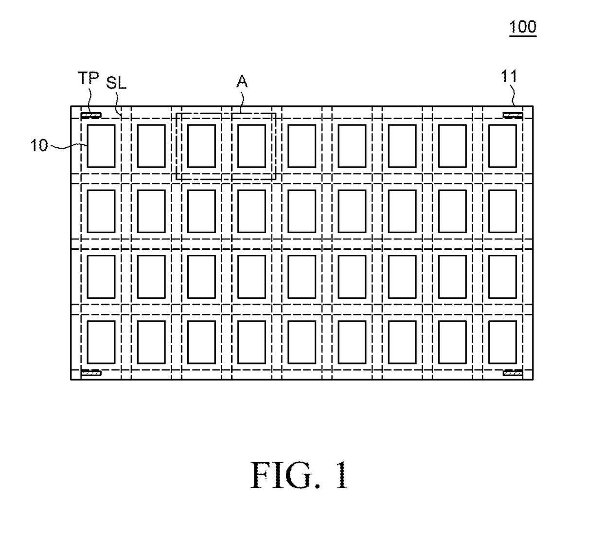
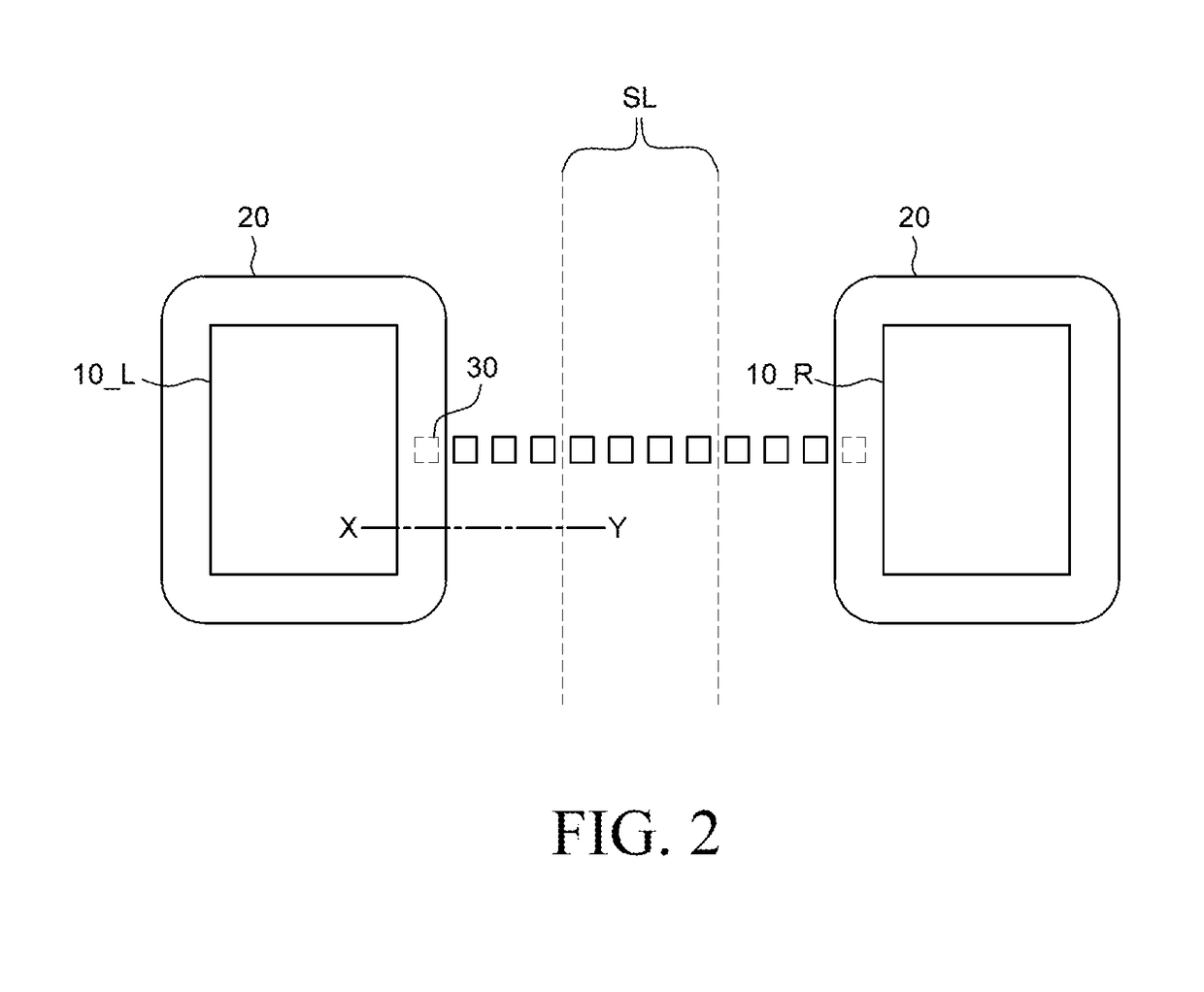
[0036]Advantages and features of the present disclosure and methods to achieve them will become apparent from the descriptions of aspects herein below with reference to the accompanying drawings. However, the present disclosure is not limited to aspects disclosed herein but may be implemented in various different ways. The aspects are provided for making the disclosure of the present disclosure thorough and for fully conveying the scope of the present disclosure to those skilled in the art. It is to be noted that the scope of the present disclosure is defined only by the claims.

[0037]The figures, dimensions, ratios, angles, the numbers of elements given in the drawings are merely illustrative and are not limiting. Like reference numerals denote like elements throughout the descriptions. And, in describing the present disclosure, descriptions on well-known technologies may be omitted in order not to unnecessarily obscure the gist of the present disclosure. It is to be noticed that th...


PUM


Abstract

Disclosed herein is a method for inspecting a transparent film. The method comprises irradiating an inspection target with light using a polarizer, receiving light that is reflected by the inspection target and passes through an analyzer by a line scan camera, synthesizing an amplitude and a phase of wavelength of the light into an intensity of light, comparing the intensity of the light with predetermined intensities of light for inspection targets having different thicknesses; and detecting a defect of the inspection target based on the compared intensity with the predetermined intensities. It can be determined whether there is a transparent film, and the thickness of the transparent film can be measured in a large area. The inspection is carried out in real-time after the transparent film is formed, such that if a defect is generated, it can be fed back immediately to thereby reduce defects. In this case, the processing cost can be saved.

Description

CROSS-REFERENCE TO RELATED APPLICATION[0001]This application claims the priority of Korean Patent Application No. 10-2016-0182989 filed on Dec. 29, 2016, in the Korean Intellectual Property Office, the disclosure of which is incorporated herein by reference in its entirety.BACKGROUNDField of the Disclosure[0002]The present disclosure relates to an inspection apparatus and an inspection method using the apparatus, and more specifically, to an inspection apparatus for determining on existence of a residual layer of a transparent film formed on a substrate for an organic light emitting panel and for measuring the thickness, and an inspection method using the apparatus.Description of the Background[0003]Display devices provide a variety of information graphically on a screen and are the core technology of the era of information and communications. Such display devices are becoming thinner, lighter and portable, along with higher performance. Among them, an organic light emitting display...

Claims


Application Information

Patent Timeline
IPC IPC(8): G01N21/958G01N21/21G01B11/06G01N21/84
CPCG01N2201/101G01N2201/0683G01N21/958G01N21/21G01B11/06G01N21/8422G01N2021/1748G01B11/0658G01N2021/8427G01B11/0625G01B11/0641G01N21/95G01N2021/8848G01N2021/8433Y02E10/549H10K59/131H01L22/12H10K71/70H10K77/111H10K50/844H10K71/851H10K71/861H10K2102/351H10K71/00
Inventor HWANG, SEOKJU
Owner LG DISPLAY CO LTD
Why Eureka
Try Eureka