Package substrate comprising side pads on edge, chip stack, semiconductor package, and memory module comprising same

Active Publication Date: 2018-07-26
SONG YOUNG HEE +3
View PDF7 Cites 11 Cited by
  • Summary
  • Abstract
  • Description
  • Claims
  • Application Information

AI Technical Summary

Benefits of technology

[0014]According to a configuration of the present invention, the following effects can be expected.
[0015]First, since memory semiconductor dies are not forcedly vertically arranged but are divided into a plurality of chip stacks and packaged, yield reduction caused by vertical stacking of the semiconductor dies can be fundamentally prevented.
[0016]Second, since a substrate is inserted into the middle between a plurality of memory semiconductor dies and the divided packages are elec

Problems solved by technology

Therefore, the miniaturization of electronic portable devices and various functions of mobile products cannot be satisfied only by simple chip stacking technology or package stacking technology.
However, in consideration of mass productivity, the number of dies 14 that can be stacked is largely limited.
The fact causes capacity limitations in implementin

Method used


Image

  • Package substrate comprising side pads on edge, chip stack, semiconductor package, and memory module comprising same
  • Package substrate comprising side pads on edge, chip stack, semiconductor package, and memory module comprising same
  • Package substrate comprising side pads on edge, chip stack, semiconductor package, and memory module comprising same

Examples


Embodiment Construction

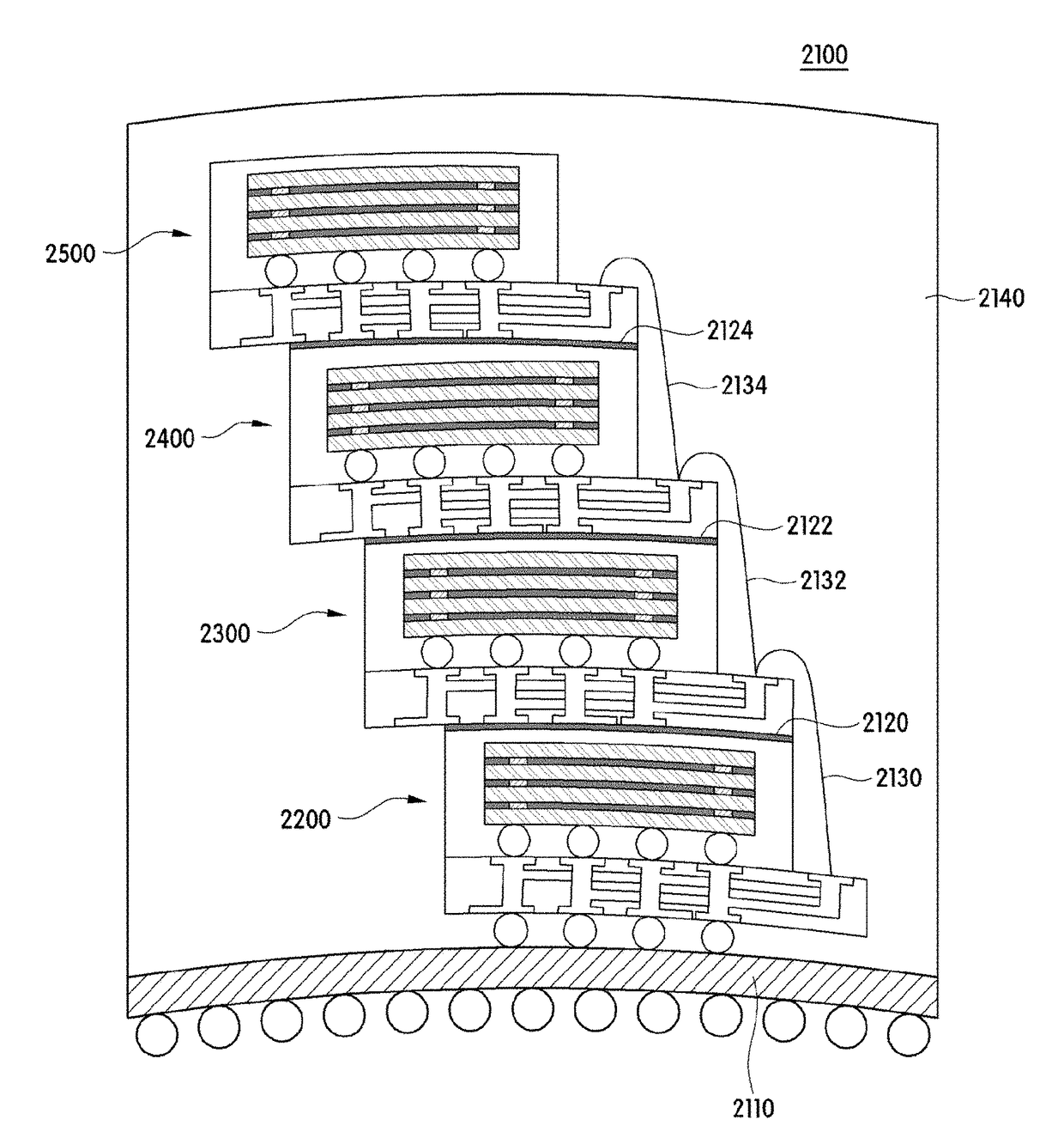
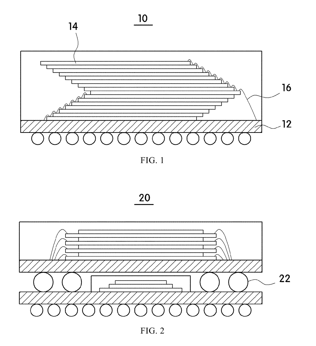
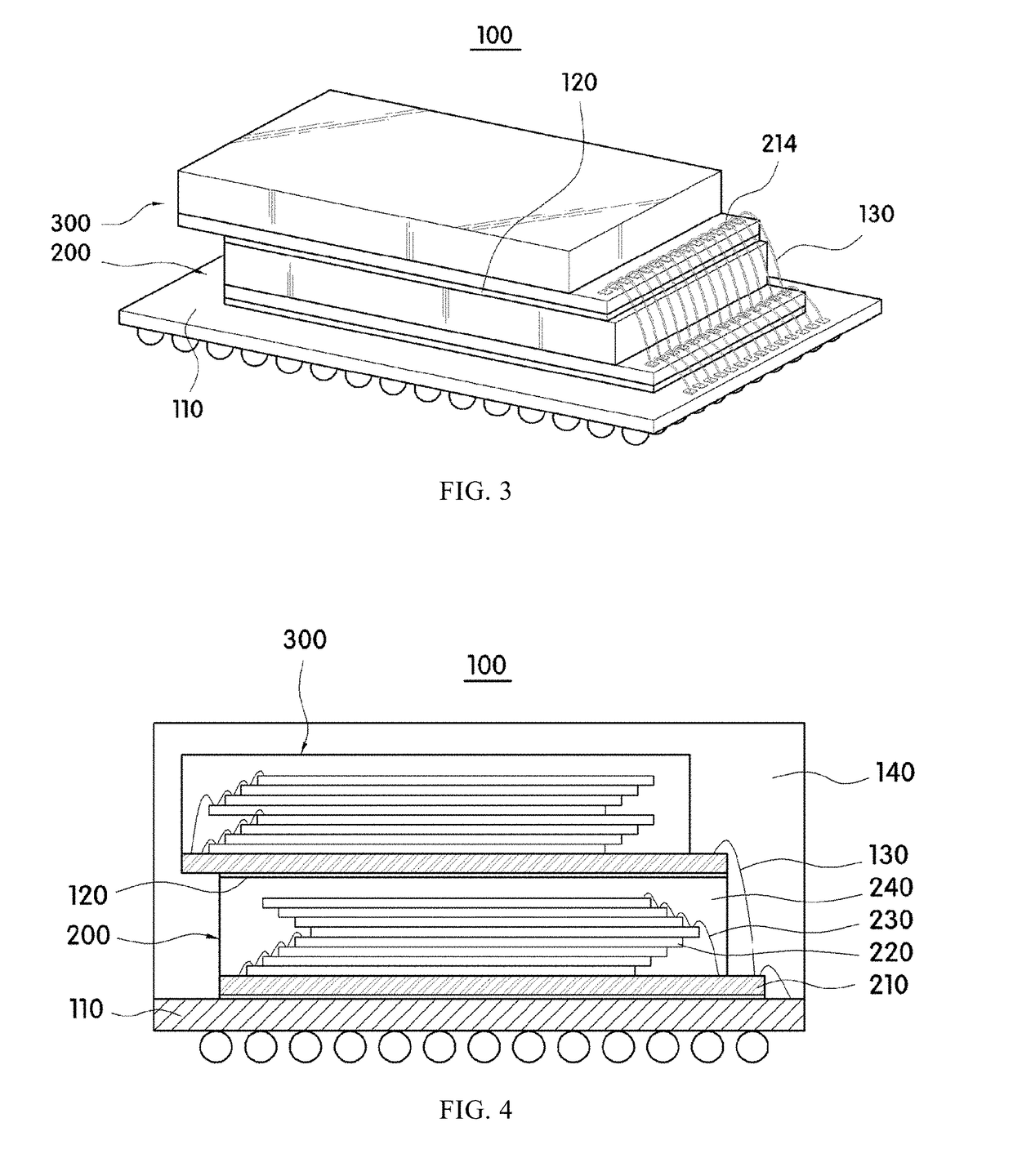
[0030]Advantages and characteristics of the present invention and a method of achieving the advantages and characteristics will be clear by referring to exemplary embodiments described below in detail together with the accompanying drawings. However, the present disclosure is not limited to the following exemplary embodiments but may be implemented in various different forms. The exemplary embodiments are provided only to complete disclosure of the present disclosure and to fully provide a person having ordinary skill in the art to which the present disclosure pertains with the category of the disclosure, and the present disclosure will be defined by the appended claims. In the drawings, a size and a relative size of a layer or an area may be exaggerated for clarity of description. Like reference numerals indicate like components throughout the specification.

[0031]The exemplary embodiments of the invention will be described with reference to plan views and cross-sectional views, whi...


PUM


Abstract

The semiconductor package according to the present invention comprises: an integrated substrate; a bottom chip stack, which is mounted on the integrated substrate, has multiple memory semiconductor dies stacked chip-on-chip, and takes charge of a part of the whole memory capacity; at least one top chip stack, which is mounted on the bottom package, has multiple memory semiconductor dies mounted therein, and takes charge of the rest of the whole memory capacity; an integration wire for electrically connecting the bottom chip stack and the top chip stack(s); and an integration protection member for sealing the integration wire.

Description

TECHNICAL FIELD[0001]The present invention relates to a package substrate including side pads on an edge, a chip stack, and a semiconductor package, and a memory module, and more particularly, to a semiconductor package in which, with a trend of standardization of solid-state drive (SSD), it is necessary to provide a high-capacity and high-speed service despite slimness and miniaturization of a package, a land grid array (LGA) type NAND flash memory semiconductor package which is most suitable to the above service is realized, packaging is firstly performed using divided chip stacks even when memory capacity required in the future increases twice, multiple types of memory chip stacks are integrally packaged in a method in which respect substrates are bonded by wire bonding using side pads on a side surface of an LGA package substrate, and thus requirements of slimness and miniaturization are satisfied even when the same area is used.BACKGROUND ART[0002]Recently, as functions of elec...

Claims


Application Information

Patent Timeline
IPC IPC(8): H01L25/10H01L25/065H01L23/00
CPCH01L25/105H01L25/0657H01L24/48H01L2225/06506H01L2225/06562H01L2225/06586H01L2224/48145H01L2224/48091H01L2225/0651H01L2224/48227H01L2225/1058H01L2225/06555H01L2224/49176H01L2225/1052H01L2924/1436H01L2225/06548H01L2225/1023H01L2924/37001H01L24/05H01L2224/04042H01L24/03H01L2224/0331H01L24/32H01L2224/32145H01L24/73H01L2224/73265H01L2924/181H01L2224/484H01L2924/15311H01L2924/19107H01L25/03H01L25/50H01L2224/16145H01L2224/16227H01L2224/32225H01L2225/06517H01L2924/15192H01L2225/06513H01L2225/06558H01L2225/06565H01L24/16H01L24/17H01L2224/17181H01L2224/4824H01L2224/73204H01L2924/15331H01L23/13H01L23/49816H01L23/5385H01L2225/1064H01L23/3128H01L23/3135H01L2924/00014H01L2924/00012H01L2924/00H01L2224/16225H01L23/28H01L23/488
Inventor SONG, YOUNG HEELEE, HYOUKSONG, KI HONGJEONG, JUN HEEYUN, SUNG SIK
Owner SONG YOUNG HEE
Why Eureka
Try Eureka