
Electrical connector

a technology of electrical connectors and solder balls, which is applied in the direction of fixed connections, coupling device connections, printed circuit manufacturing, etc., can solve the problems of wasting energy and time to completely melt solders, irregular shape of solder balls, and bad situations of missing solders, so as to reduce energy consumption, shorten the soldering period, and control accurately

Active Publication Date: 2018-07-26
LOTES
View PDF4 Cites 5 Cited by
  • Summary
  • Abstract
  • Description
  • Claims
  • Application Information

AI Technical Summary

Benefits of technology

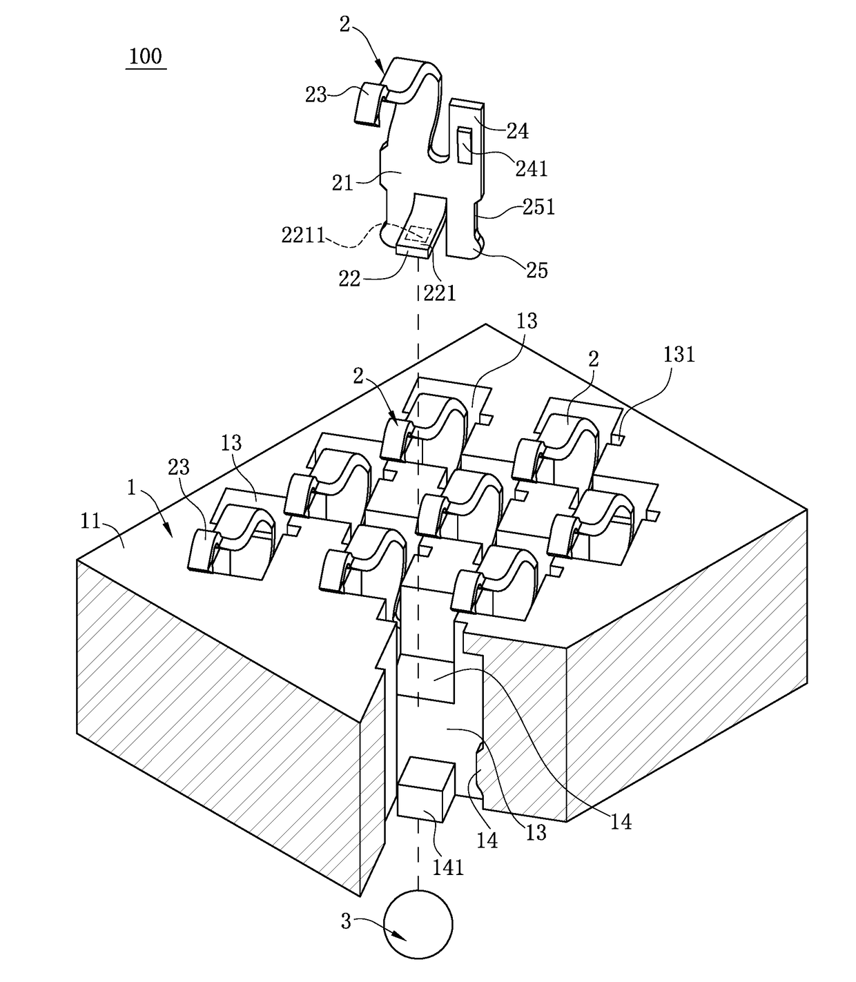
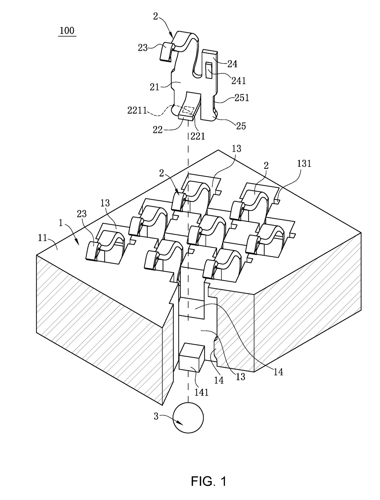
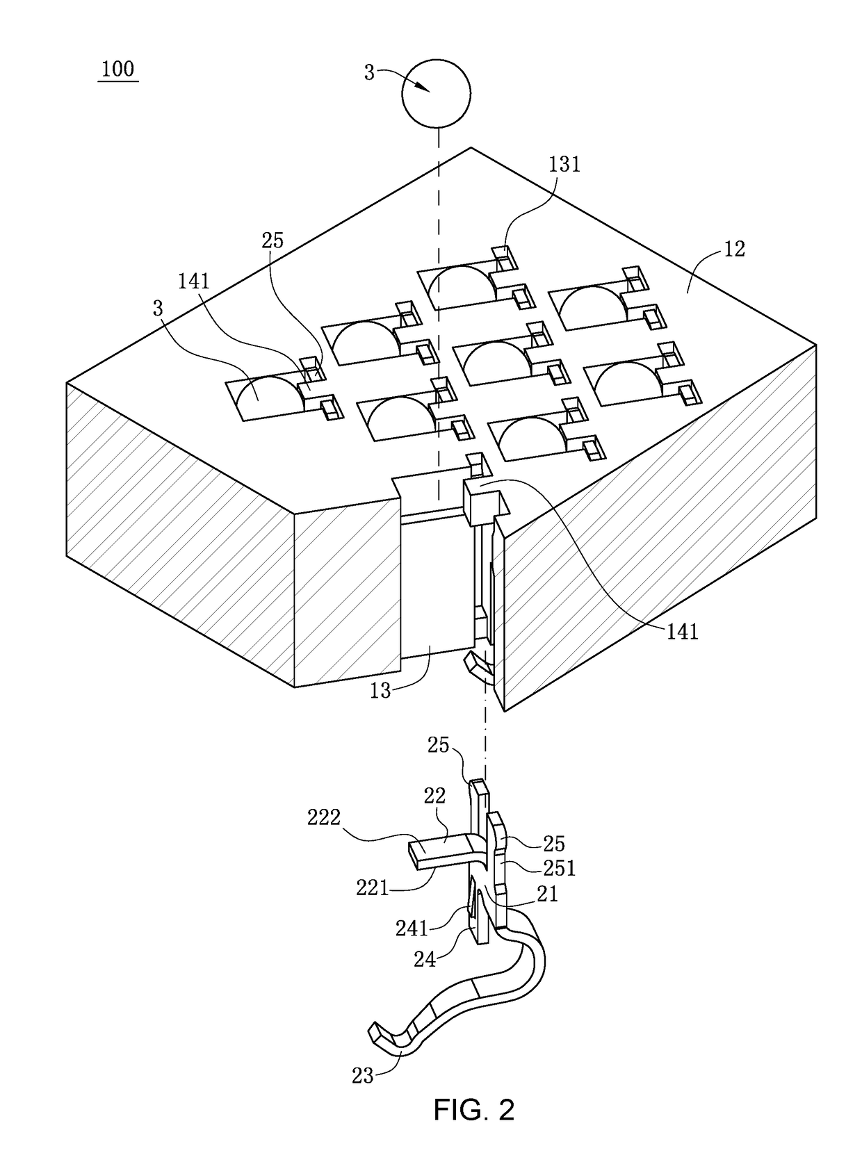
The present invention relates to a new electrical connector that addresses issues of inconsistent solder shape and size during soldering. The connector uses external laser to solder terminals and solders, ensuring consistent shape and size of the solder. Additionally, the connector has a through hole that acts as a heating mechanism, allowing for controlled and direct energy heating of the solder, reducing energy consumption and cost. The technical effects of the present invention include improved quality of soldering, reduced energy consumption, and cost savings.

Problems solved by technology

However, energy and time are consumed to completely melt solders, and moreover, the heights of the solders are not in the same plane due to inconsistent solidification shape of the solders, thereby causing bad situations of missing solder and the like during soldering of an electrical connector and a circuit board.
However, the contact area is over-narrow and over-small, laser soldering is within a controllable precision range, but a laser beam will still deviate from the contact area, irradiate other parts of solder balls, or deviate from the solder balls, causing irregular shaped solder balls, inconsistent heights of the solder balls, or missing solder, thereby influencing soldering of the electrical connector and the circuit board.
Therefore, a heretofore unaddressed need exists in the art to address the aforementioned deficiencies and inadequacies.

Method used


Image

  • Electrical connector
  • Electrical connector
  • Electrical connector

Examples


Embodiment Construction

[0058]The present invention is more particularly described in the following examples that are intended as illustrative only since numerous modifications and variations therein will be apparent to those skilled in the art. Various embodiments of the invention are now described in detail. Referring to the drawings, like numbers indicate like components throughout the views. As used in the description herein and throughout the claims that follow, the meaning of “a”, “an”, and “the” includes plural reference unless the context clearly dictates otherwise. Also, as used in the description herein and throughout the claims that follow, the meaning of “in” includes “in” and “on” unless the context clearly dictates otherwise. Moreover, titles or subtitles may be used in the specification for the convenience of a reader, which shall have no influence on the scope of the present invention.

[0059]It will be understood that when an element is referred to as being “on” another element, it can be di...


PUM


Abstract

An electrical connector is used for electrically connecting a chip module to a circuit board. The electrical connector includes an insulating body having multiple receiving holes and multiple terminals received in the receiving holes The electrical connector has a top surface and a bottom surface The receiving holes run through the insulating body. Each terminal has a base and a soldering portion extending from a lower part thereof. Two opposite sides of the soldering portion are a first surface and a second surface. The first surface includes a laser irradiation area. A solder is provided at a position, opposite to the laser irradiation area, of the second surface for urging. The laser irradiation area is heated by external laser, such that the solder is partially melted and is soldered and fixed to the second surface.

Description

CROSS-REFERENCE TO RELATED APPLICATION[0001]This non-provisional application claims priority to and benefit of, under 35 U.S.C. § 119(a), Patent Application No. 201720072288.2 filed in P.R. China on Jan. 20, 2017, the entire content of which is hereby incorporated by reference.FIELD OF THE INVENTION[0002]The present invention relates to an electrical connector, and more particularly to an electrical connector that electrically connects a chip module to a circuit board.BACKGROUND OF THE INVENTION[0003]Chinese Patent Application No. CN201210359807.5 discloses an electrical connector. The electrical connector includes a housing and an electrical terminal mounted on the housing. The electrical connector is surface mounted on a circuit substrate. The electrical terminal has a substrate connecting portion soldered to the circuit substrate. The substrate connecting portion is formed in a rectangular plate shape extending in a length direction and a width direction, and has a surface opposi...

Claims


Application Information

Patent Timeline
Patent Type & Authority Applications(United States)
IPC IPC(8): H01R12/57H01R12/72H01R4/02H01R13/518H05K3/34
CPCH01R12/57H01R12/721H01R12/725H01R4/02H01R13/518H05K3/3436H01R12/716H01R43/0221
Inventor CHANG, WEN CHANGJIN, ZUO FENG
Owner LOTES
Learn More