Array substrate, liquid crystal display panel and manufacturing method

a technology of liquid crystal display panel and array substrate, which is applied in the field of array substrate, liquid crystal display panel and manufacturing method, can solve the problems of high cost and complex manufacturing process above, and achieve the effect of reducing three masking and increasing conductivity

Active Publication Date: 2018-08-02
WUHAN CHINA STAR OPTOELECTRONICS TECH CO LTD
View PDF0 Cites 11 Cited by
  • Summary
  • Abstract
  • Description
  • Claims
  • Application Information

AI Technical Summary

Benefits of technology

[0017]Beneficial effects of the disclosure are distinguishing from the prior art, the data line layer and the light shield layer are designed on a same layer according to the disclosure, moreover, the source electrode, the drain electrode, the oxide semiconductor layer and the common electrode layer are designed on a same layer, the source electrode layer, the drain electrode layer and the common electrode layer are formed by doping the oxide semiconductor material, material of the source electrode layer, the drain electrode layer and the common electrode layer can be conductive by increasing conductivity thereof, which can reduce three masking processes compared with the prior art, only 5 masks are required, which can reduce the amount of masks in the process significantly and costs in production.

Problems solved by technology

However, the oxide semiconductor TFT is sensitive to light, an additional light shield layer is required to reduce influence of light on stability of a device.
The manufacturing process above is pricy and complex due to the additional amount of masks.

Method used


Image

  • Array substrate, liquid crystal display panel and manufacturing method
  • Array substrate, liquid crystal display panel and manufacturing method
  • Array substrate, liquid crystal display panel and manufacturing method

Examples


Embodiment Construction

[0024]Embodiments of the disclosure will be described in detail with reference to the accompanying drawings as follows.

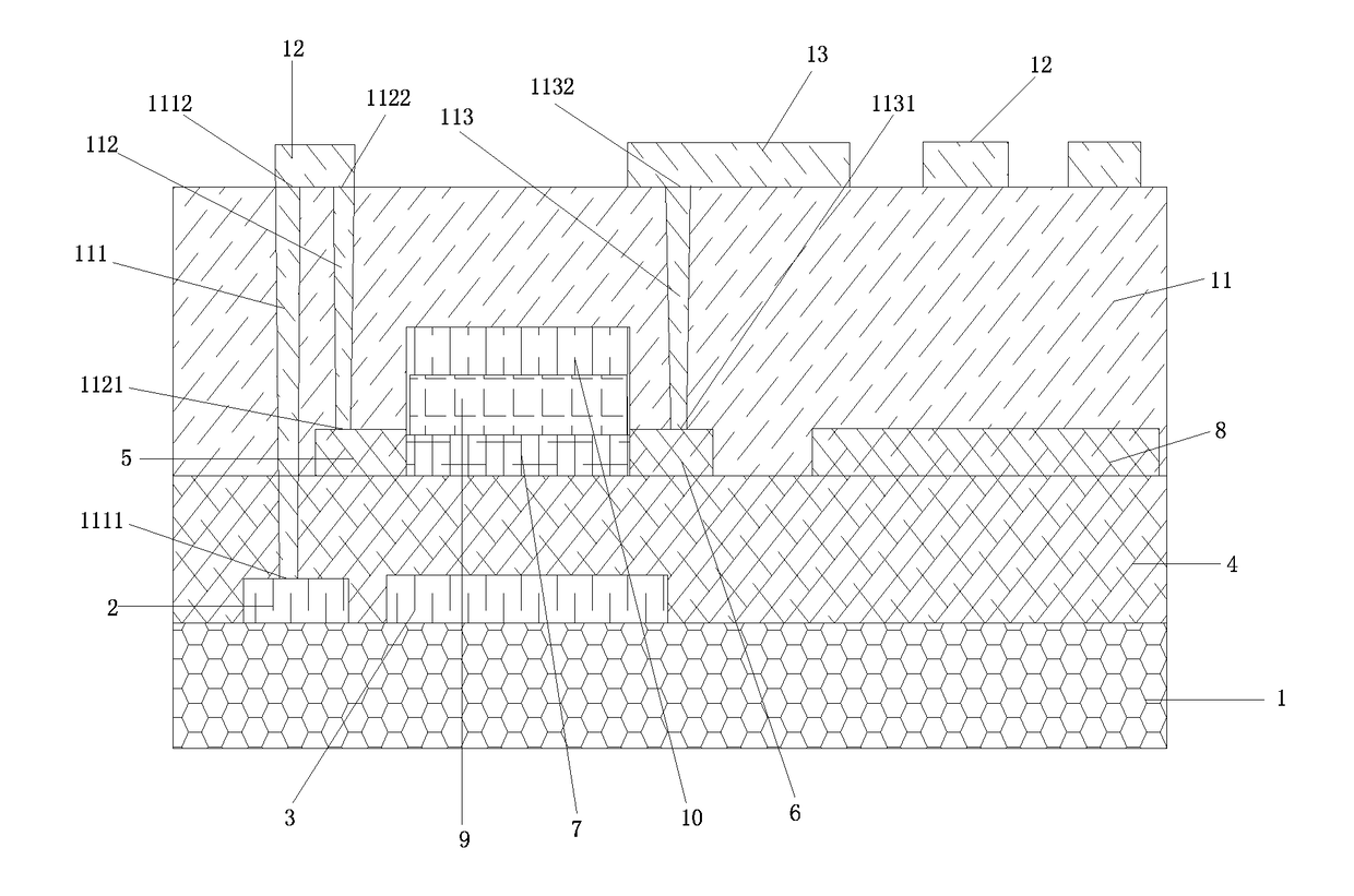
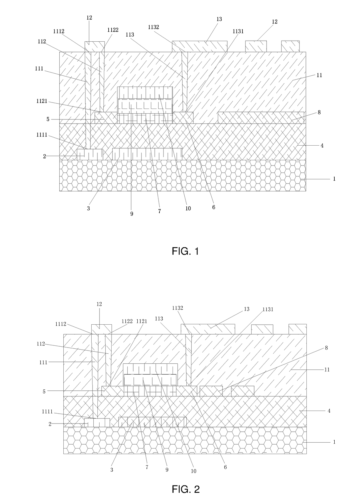
[0025]Referring to FIG. 1 and FIG. 2, FIG. 1 and FIG. 2 are structural schematic views of array substrates according to two embodiments of the disclosure, the array substrate includes a substrate 1, a data line layer 2, a light shield layer 3, a first insulating layer 4, a source electrode layer 5, a drain electrode layer 6, an oxide semiconductor layer 7, a common electrode layer 8, a second insulating layer 9, a gate electrode layer 10, an interlayer deposition 11, a transparent electrode layer 12 and a pixel electrode layer 13.

[0026]The data line layer 2 and the light shield layer 3 are in a same layer, which are formed on the substrate 1 separately, material of the light shield layer 3 and that of the data line layer 2 are both metallic material. In other words, a difference compared with the prior art is that the data line layer 2 and the light shield layer 3 a...


PUM

PropertyMeasurementUnit
conductiveaaaaaaaaaa
transparentaaaaaaaaaa
metallicaaaaaaaaaa

Abstract

The disclosure discloses an array substrate, a liquid crystal display panel and a manufacturing method, the array substrate includes designing a data line layer and a light shield layer on a same layer, moreover, a source electrode layer, a drain electrode layer, an oxide semiconductor layer and a common electrode layer are designed on a same layer, the source electrode layer, the drain electrode layer and the common electrode layer are formed by doping the oxide semiconductor material, the source electrode layer, the drain electrode layer and the common electrode layer can be conductive by increasing conductivity thereof. By the method above, the disclosure can reduce the amount of masks in processes and costs in production significantly.

Description

TECHNICAL FIELD[0001]The disclosure relates to a liquid crystal display technical field, and more particularly to an array substrate, a liquid crystal display panel and a manufacturing method.DESCRIPTION OF RELATED ART[0002]An oxide semiconductor TFT is becoming a serious competitor in a next generation of display technique due to advantages such as high mobility and mass production.[0003]However, the oxide semiconductor TFT is sensitive to light, an additional light shield layer is required to reduce influence of light on stability of a device. In the prior art, during manufacturing an oxide semiconductor TFT liquid crystal display panel, an extra masking step is required to add the light shield layer, therefore, 8 masking processes are generally required for the entire device.[0004]The manufacturing process above is pricy and complex due to the additional amount of masks.SUMMARY[0005]The disclosure provides an array substrate, a liquid crystal display panel and a manufacturing met...

Claims


Application Information

Patent Timeline
Patent Type & Authority Applications(United States)
IPC IPC(8): G02F1/1362H01L27/12H01L29/786G02F1/1343G02F1/1368
CPCG02F1/136209H01L27/1225H01L27/124H01L27/127H01L27/1288H01L29/78633H01L29/7869G02F1/13439G02F1/136286G02F1/1368G02F1/134363G02F2001/136295G02F2001/136231G02F2202/06G02F2202/10G02F2001/13685G02F1/136227G02F2001/134318G02F1/136231G02F1/136295G02F1/13685G02F1/134318
Inventor XIE, YINGTAO
Owner WUHAN CHINA STAR OPTOELECTRONICS TECH CO LTD
Why Eureka
Try Eureka