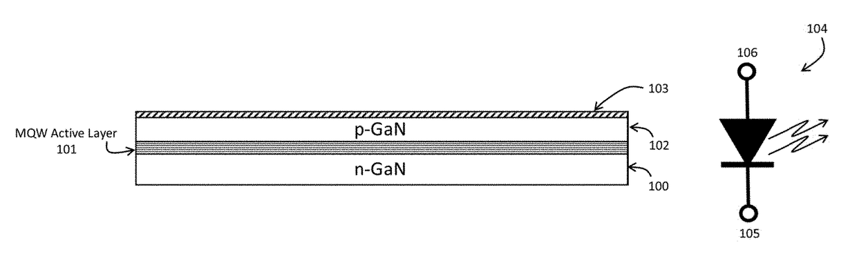
[0148]REFF is the effective coupling shunt resistance (Ohms)
[0156]The DC bias is set by adjusting voltage source 1607 to a preset positive potential Vpos to bias the LED devices through the load resistor RL 1608, field plate contact 1609, gap medium 1606, through the LED devices to bottom contact 1604. To achieve the DC bias point of 10 mA / cm2, a total current of 50 mA must flow through RL. If RL is chosen as 100 kohm to allow an efficient coupling of an AC pulse through coupling capacitor CC 1610 roughly 5 kV positive bias Vpos is needed. The voltage drop through the DI water is about 25V while the LED requires 2.5-3.5V to turn on. Note that by varying the bias level, a graph of the output light level versus DC current density bias can be measured. Pulsing the DC bias synchronously with the camera capture time would allow signal averaging and multiple device bias set points to be measured.
[0157]A pulsed signal response can be combined by pulsing source 1611 through coupling capacitor 1610. Assuming a CL of 1 nF, a fast pulse can couple charge into the LED devices before RL×CC relaxation can lower the charge coupling efficiency. For 100 kohm and 1 nF device values, the system relaxation time constant is 100 μsec, a value sufficiently long to ensure that the charge can be transferred to the LED devices and converted to a measurable pulse of light. In this example, the total DI water coupling capacitance is about 14 nF. If a 100 mA / cm2 bias is injected for 5 μsec, a total charge of about 3 pC per LED device or 2.4 μC for the test area must be delivered. Since the DI coupling capacitor is about 14 nF, the effective coupling capacitance would still be about 1 nF. The voltage pulse magnitude required of source 1611 would be 2400 volts ramped in 5 μsec. This way, both DC biasing and AC pulsed functional test can be made of an LED device substrate with a bottom common contact. Of course, there can be other bias and pulsing configurations, variations, modifications, and alternatives.
[0158]Although this invention has been described with a common contact existing under the LED devices, other device of injecting current are possible. FIG. 17A shows another embodiment 1700 where an analogue to the field plate 1701 is present within support substrate 1702 below the plurality of LED device structures such as LED device 1703. Under the lowest LED device structure layer (the n-layer in examples described in this invention), a dielectric layer 1704 and electrode 1705 completes the support substrate capacitive coupling device. Electrode 1705 is connected to a voltage source 1706. The field plate is connected to a separate voltage source 1707 and field plate electrode 1708. In this example, a camera 1709 is placed above the field plate to capture the light emission response of the plurality of LED devices under test. In this example, the isolation between devices is shown to be complete, however this method would still function with or without full isolation of the n-layer. FIG. 17B shows the equivalent circuit 1711 of this capacitively coupled support substrate configuration. The only change is the insertion of a second coupling capacitor CEFF2 below each LED device cathode. The resulting circuit can be made to operate equivalently and be effective in performing C2I functional test. For example, assuming a support substrate dielectric layer 1704 identical to dielectric layer 1710 within the field plate, voltage source 1706 driven identically but negatively to voltage source 1707 (0 to −500V for source 1706 and 0 to +500V for source 1707), the measurement system 1700 would perform essentially identically to a common contact support substrate configuration.
[0159]In yet another embodiment, C2I functional testing could also be applied to a modification of the test configuration of FIG. 17A that eliminates the need for a buried electrode within the support substrate. In this embodiment, the dielectric property of the support substrate itself is used to inject current through the LED devices. For example, a quartz, sapphire, glass or plastic support substrate could serve as dielectric 1704 in FIG. 17A. FIG. 18 shows a specific embodiment 1800 of this configuration. A support substrate 1801 having adequate dielectric properties and thickness containing a plurality of LED devices on its surface such as LED device 1802 is placed on top of an electrode 1803 connected to a voltage source 1806. Although not shown specifically, a gap can exist between electrode 1803 and support substrate 1801, allowing non-contact operation of the back side of the support substrate if desired. Although not shown specifically, an additional dielectric can also be interposed between electrode 1803 and support substrate 1801. The gap (and optional dielectric covering electrode 1803) will modify CEFF2 in a similar manner as the top field plate to device gap 509 modified CEFF & CEFF′ using equations 2-4. Field plate 1804 having a dielectric layer 1805 and electrode 1806 connected to a second voltage source 1807 completes the C2I functional test circuit. A camera 1808 placed above field plate 1804 is shown in this embodiment. The equivalent electrical circuit would be similar to FIG. 17B except that the value CEFF2 is likely substantially smaller due to the thickness of the support substrate. For example, a support substrate made of sapphire (εr˜10) of 500 μm in thickness, C′EFF2 will be approximately 18 pF / cm2, about 65 times smaller than CEFF1. A faster voltage ramp and / or a larger voltage value for V1 could compensate for this loss of coupling efficiency. For example, field plate voltage source 1807 could be driven from 0 to +500V while the support substrate voltage source 1804 could be driven at 0 to −32.5 kV (−500V×65=−32.5 kV). The electric field strength within the sapphire support substrate would be 0.65 MV / cm, well below its breakdown strength of approximately 1 MV / cm. Driven in this fashion, the LED devices would be driven substantially equivalently and allow C2I functional test without a buried contact within the LED device support substrate. High-voltage waveform generators to drive electrode 1803 can be realized using IGBT, MOSFET, or thyristor devices. High-voltage switches capable of switching up to 36 kV are model number HTS-361-01-C (36 kV, 12 A max current) and model number HTS-361-200-FI (36 kV, 2000 A max current) from Belke Electronic GMBH (Kronberg, Germany). Programmable waveform shaping circuits could slow the fast voltage change to a voltage ramp meeting the desired C2I functional test properties. For a 6″ substrate, the total capacitance would be about 3.2 nF and at 16 measurements per seconds, the ½ CV2f power would be about 27 Watts and the average current would be 830 μA, safely within normal operating specifications for commercially available high-voltage switches. For the HTS-361-200-FI 2000 A capable switch, current density C2I measurements as high as 11 A / cm2 could be performed. Of course, there can be other variations, modifications, and alternatives.