Silicon substrate processing method and liquid ejection head manufacturing method

Active Publication Date: 2018-09-20
CANON KK
View PDF0 Cites 0 Cited by
  • Summary
  • Abstract
  • Description
  • Claims
  • Application Information

AI Technical Summary

Benefits of technology

[0005]A silicon substrate processing method according to an aspect of the present disclosure includes: providing a silicon substrate with a sacrificial layer formed in a form of an island on a front surface thereof, the front surface being a surface on a side where a flow path of an ejection port for ejecting liquid is to be formed, the sacrificial layer having a higher etching rate than the silicon substrate; forming a mask layer on a back surface of th

Problems solved by technology

In such a method, since the ink flow path forming member and so on are formed on the front surface of the silicon substrate, it is impossible to apply a

Method used


Image

  • Silicon substrate processing method and liquid ejection head manufacturing method
  • Silicon substrate processing method and liquid ejection head manufacturing method
  • Silicon substrate processing method and liquid ejection head manufacturing method

Examples


Example

Example 1

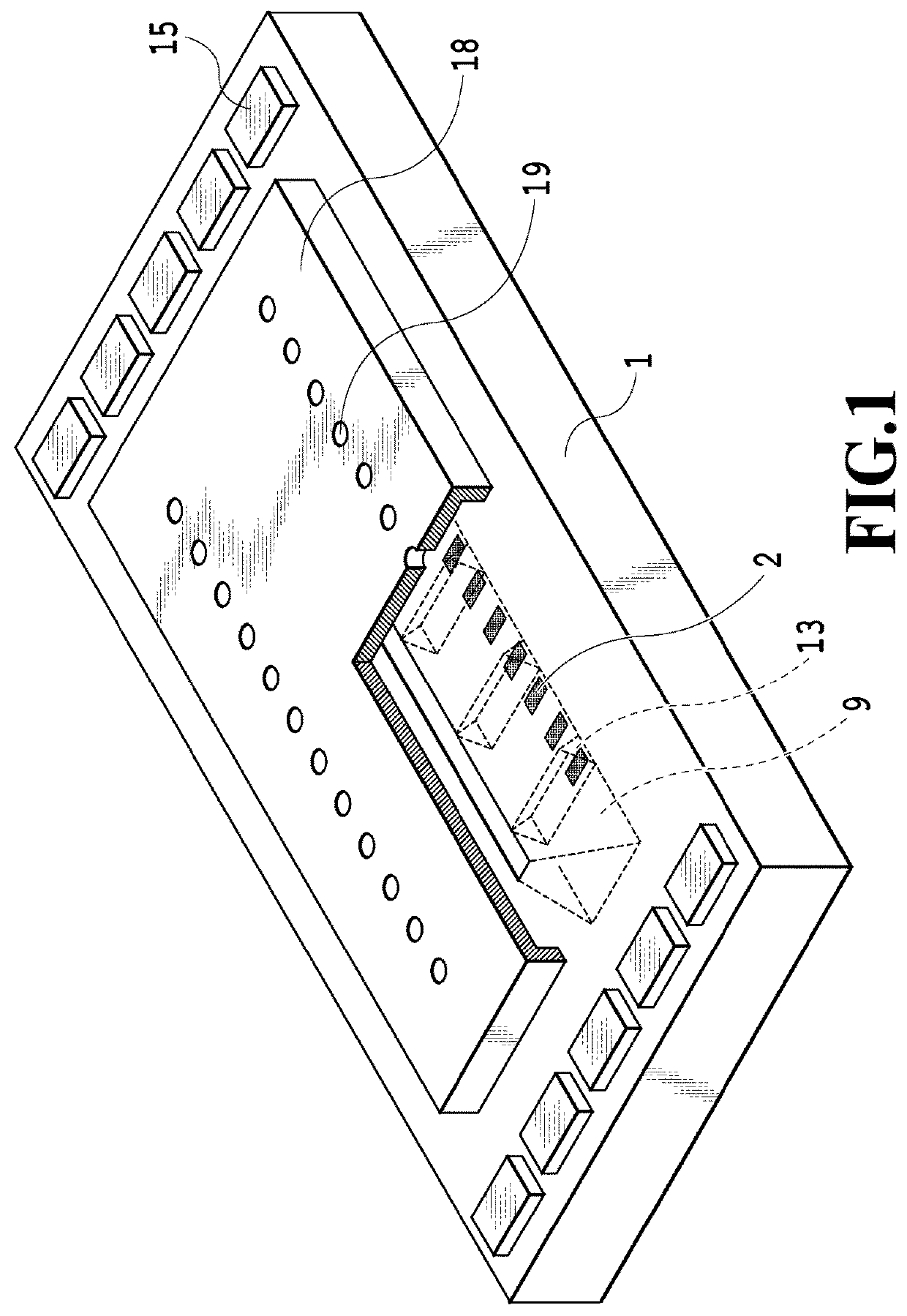
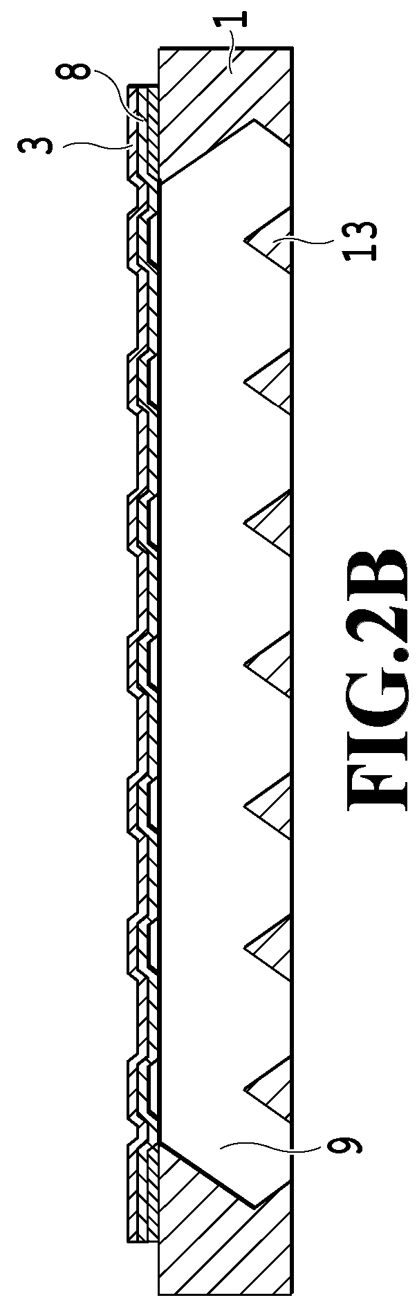
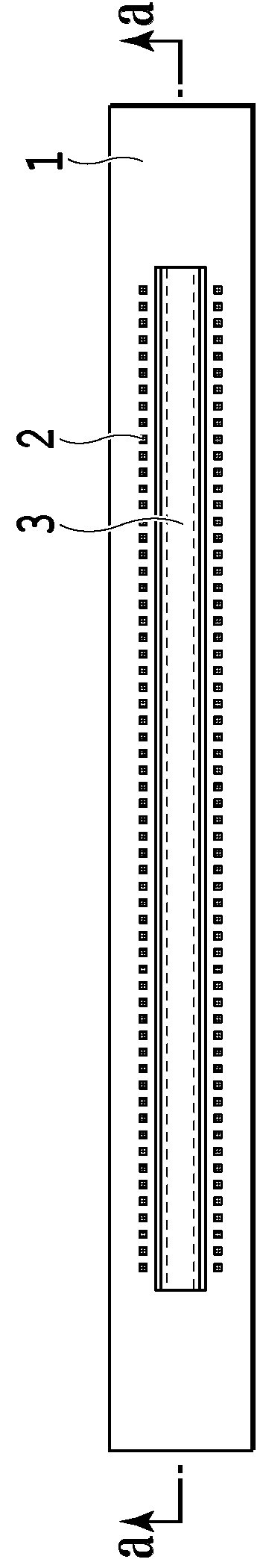
[0040]A silicon substrate 1 for an inkjet recording head is provided by following FIGS. 3A to 5D. The following operations are performed for the silicon substrate 1.

[0041]First, as illustrated in FIGS. 3A, 4A, and 5A, a sacrificial layer 6 made of an Al—Si (aluminum-silicon) alloy is formed in the form of islands on the front surface of the silicon substrate 1 within the area where an ink supply port 9 is to be formed, at the positions opposite from the portions at which beams 13 are to be formed. The dimension of each island of the sacrificial layer 6 is 430 μm. Moreover, etch-resistant plasma SiO (silicon oxide film) is formed as an etching stop layer 8 on the front surface of the silicon substrate 1. The sacrificial layer 6 and the etching stop layer 8 are formed in the same step as the step of forming electrothermal conversion elements 2, which are energy generating elements, and so on on the front surface of the silicon substrate 1. Polyamide resin is deposited on an S...


PUM


Abstract

Provided is a silicon substrate processing method including: providing a silicon substrate with a sacrificial layer formed in the form of an island on the front surface thereof, the front surface being a surface on a side where the flow path of an ejection port for ejecting liquid is to be formed, the sacrificial layer having a higher etching rate than the silicon substrate; forming a mask layer on the back surface, the back surface being a surface opposite from the front surface, the mask layer being a layer that does not include an opening at a portion of the back surface opposite from the sacrificial layer; forming a non-penetrating hole from an opening on the back surface of the silicon substrate; and forming a beam on the back surface side by performing anisotropic etching on the silicon substrate in which the non-penetrating hole is formed.

Description

BACKGROUND OF THE INVENTIONField of the Invention[0001]The present disclosure relates to a silicon substrate processing method and a liquid ejection head manufacturing method.Description of the Related Art[0002]Processing a silicon substrate by, for example, forming recesses, through holes, and surficial films has been known, and employing the processed silicon substrate for micro electro mechanical systems (MEMS), which are components of electronic devices, has been known. A silicon substrate thus processed may be used as a part of a liquid ejection head, which is employed for inkjet recording or the like. Also, forming beams inside an ink supply port formed in the silicon substrate to enhance the strength of the substrate has been known.[0003]Japanese Patent Laid-Open No. 2004-148825 describes a technique of forming an ink supply port having beams on the back surface of a substrate. The technique described in Japanese Patent Laid-Open No. 2004-148825 is as follows. A mask is forme...

Claims


Application Information

Patent Timeline
IPC IPC(8): B41J2/16C30B29/06B41J2/14
CPCB41J2/1629C30B29/06B41J2/1433B41J2202/22
Inventor KISHIMOTO, KEISUKE
Owner CANON KK
Why Eureka
Try Eureka