
Etching control method

A control method and technology to be etched, applied in semiconductor/solid-state device manufacturing, electrical components, circuits, etc., and can solve problems such as poor electrical performance of chips

Pending Publication Date: 2021-03-19
BEIJING NAURA MICROELECTRONICS EQUIP CO LTD
View PDF0 Cites 0 Cited by
  • Summary
  • Abstract
  • Description
  • Claims
  • Application Information

AI Technical Summary

Problems solved by technology

However, the chip obtained by using DBR often has the problem of poor electrical performance of the chip.

Method used


Image

  • Etching control method
  • Etching control method
  • Etching control method

Examples


Embodiment Construction

[0030] The present application is described in detail below, and examples of embodiments of the present application are shown in the drawings, wherein the same or similar reference numerals denote the same or similar components or components having the same or similar functions throughout. Also, detailed descriptions of known technologies will be omitted if they are not necessary to illustrate the features of the present application. The embodiments described below by referring to the figures are exemplary only for explaining the present application, and are not construed as limiting the present application.

[0031] Those skilled in the art can understand that, unless otherwise defined, all terms (including technical terms and scientific terms) used herein have the same meanings as commonly understood by those of ordinary skill in the art to which this application belongs. It should also be understood that terms, such as those defined in commonly used dictionaries, should be ...


PUM


Abstract

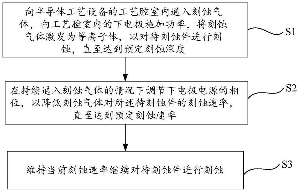
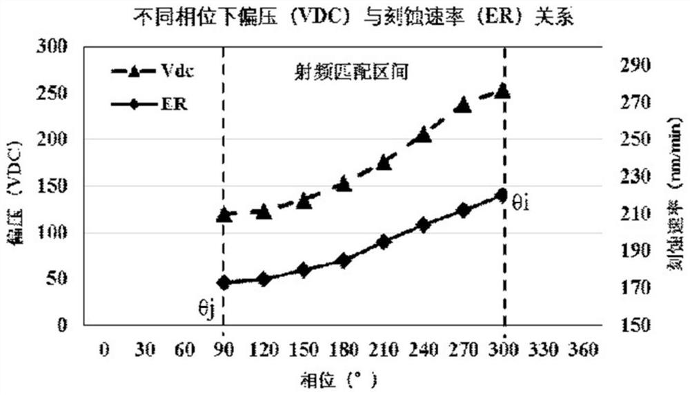
The invention provides an etching control method, and the method comprises a main etching step: introducing etching gas into a technological cavity of semiconductor technological equipment, applying power to a lower electrode in the technological cavity, and enabling the etching gas to be excited into plasma, so as to etch a to-be-etched part till the to-be-etched part reaches a preset etching depth; a transition etching step: adjusting the phase of the lower electrode power supply under the condition of continuously introducing the etching gas so as to reduce the etching rate of the etching gas on the to-be-etched part until the preset etching rate is reached; and an over-etching step: maintaining the current etching rate to continue the etching of the to-be-etched part. By applying the method, damage to the bottom metal layer can be reduced, and metal is prevented from being sputtered to the side wall.

Description

technical field [0001] The present invention relates to the technical field of semiconductor technology, in particular to an etching control method. Background technique [0002] In the manufacturing process of semiconductor optoelectronic devices, in order to effectively utilize the light emitted from the front of the light-emitting layer, the LED chip will be flip-chip (substrate facing up), so that the light-emitting surface is on the sapphire side, and it needs to be prepared on the surface where the electrode is located. A mirror layer. [0003] In the prior art, Ni / Ag / Au composite metal is usually used as the reflective mirror surface layer, but its light absorption is serious, and the process is complicated. The reflectivity in the blue light band is still lower than 90%, and the reflection effect on light is not very good. In order to improve the utilization rate of light and enhance the reflection effect, people have developed and designed DBR (Distributed Bragg Re...

Claims


Application Information

Patent Timeline
IPC IPC(8): H01L21/311H01L33/46H01L21/67
CPCH01L33/46H01L21/31116H01L21/67253H01L2933/0025
Inventor 国唯唯
Owner BEIJING NAURA MICROELECTRONICS EQUIP CO LTD
Learn More