Substrate etching method

A technology of substrate and main etching, applied in the direction of electrical components, semiconductor/solid-state device manufacturing, circuits, etc., can solve the problems of energy loss, small proportion of process time, and enhanced particle bombardment ability, so as to improve the height and enhance ion Bombardment energy, the effect of increasing the etching selectivity ratio

Inactive Publication Date: 2016-02-17
BEIJING NAURA MICROELECTRONICS EQUIP CO LTD
View PDF4 Cites 0 Cited by
  • Summary
  • Abstract
  • Description
  • Claims
  • Application Information

AI Technical Summary

Problems solved by technology

The upper RF system of the ICP equipment generally uses a 13.56MHz power supply, and cooperates with the helical coil to generate induction plasma; the lower RF system can use either a 13.56MHz power supply or a 2MHz power supply. Both have their own advantages and disadvantages: the former is prone to upper and lower The problem of energy loss and interference caused by radio frequency coupling; and the latter will cause the problem of insufficient bottom width of PSS graphics due to the enhanced particle bombardment ability
[0011] The over-etching step mainly plays the role of modifying the graphic morphology, and the proportion of the process time i...

Method used


Image

  • Substrate etching method
  • Substrate etching method
  • Substrate etching method

Examples


Embodiment Construction

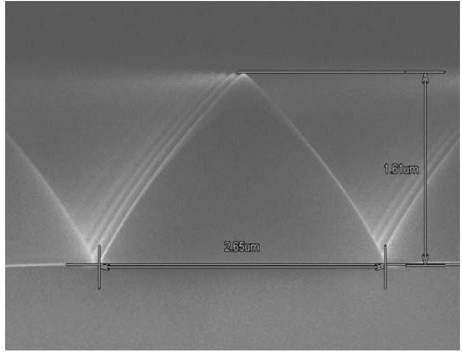
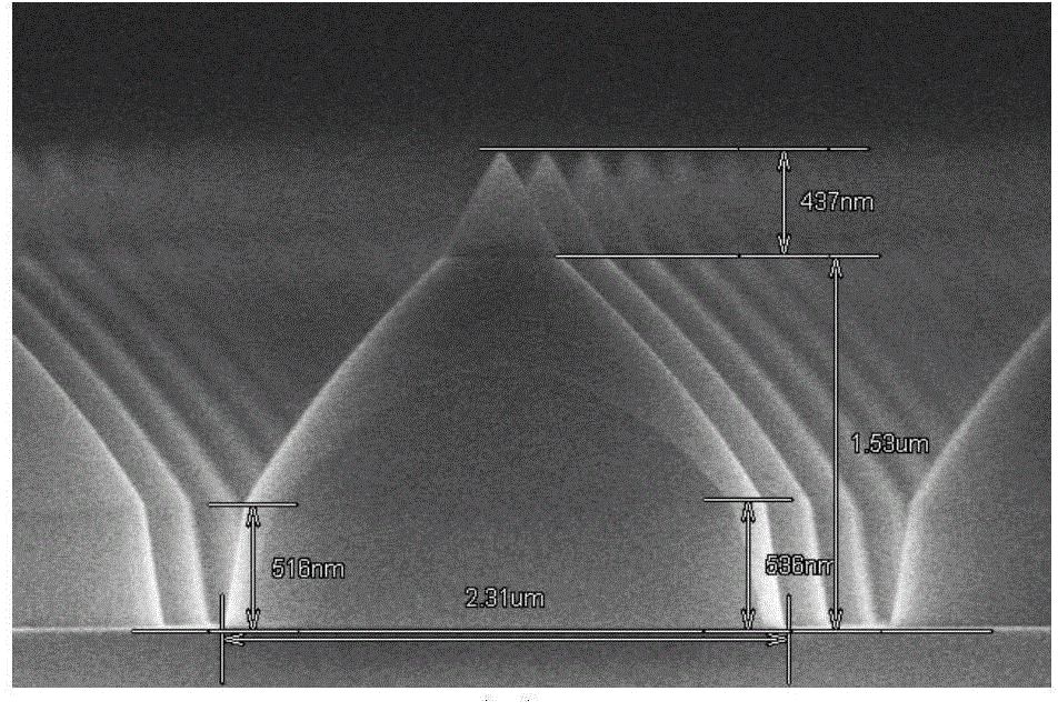
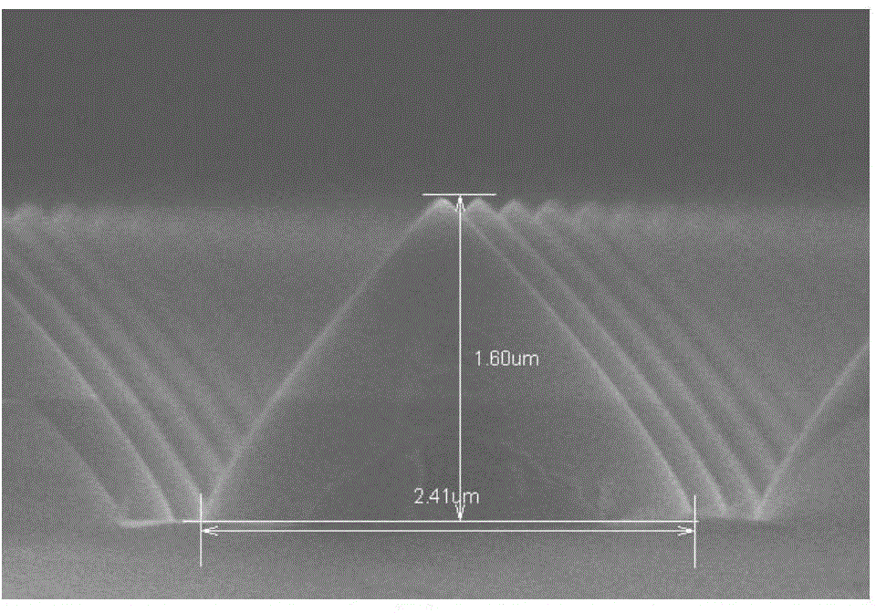
[0041] In order for those skilled in the art to better understand the technical solution of the present invention, the substrate etching method provided by the present invention will be described in detail below in conjunction with the accompanying drawings.

[0042]The substrate etching method provided by the embodiment of the present invention adopts the existing plasma processing equipment to carry out the etching process. Preferably, the plasma processing equipment can be an inductively coupled plasma equipment, which mainly includes a reaction chamber, an induction coil, an upper RF system and lower RF system. Wherein, a carrying device for carrying the substrate is provided in the reaction chamber, such as a base, a mechanical chuck or an electrostatic chuck, and the like. Moreover, a temperature control device is also provided in the reaction chamber to adjust the temperature of the substrate. In addition, during the etching process, helium gas is delivered to the gap ...


PUM


Abstract

A substrate etching method provided in the invention comprises the following steps of a main etching step: etching a graph on a substrate and increasing a bottom width of a profile graph through reducing a substrate surface temperature and lower electrode power during an etching process; an over etching step: continuously etching the substrate, increasing a height of the profile graph through increasing the substrate surface temperature and the lower electrode power and simultaneously modifying a graphic morphology. The main etching step is stopped when a mask layer begins to carry out transverse shrinkage and simultaneously the over etching step begins to carry out. By using the substrate etching method, the ideal graphic morphology can be acquired, and the bottom width and the height of the profile graph can satisfy a technology requirement.

Description

technical field [0001] The invention relates to the technical field of semiconductors, in particular to a substrate etching method. Background technique [0002] PSS (Patterned Sapphire Substrate, patterned sapphire substrate) technology is currently a relatively popular method for improving the light extraction efficiency of blue LED chips. It has been proved by production and experiments that the shape of PSS graphics has a great influence on the degree of improving the light extraction efficiency. Among them, the conical shape with straight side walls (the side section is triangular) is more and more popular because of its significant effect on improving light extraction efficiency. It has become more and more popular and has become a more popular process indicator. Generally, the ideal PSS graphic morphology requires that the height of the cross-sectional graphic (triangular) be 1.6±0.1μm, and the bottom width be 2.6±0.15μm; figure 1 shown. [0003] At present, the sa...

Claims


Application Information

Patent Timeline
IPC IPC(8): H01L21/02
Inventor 吴鑫朱印伍
Owner BEIJING NAURA MICROELECTRONICS EQUIP CO LTD
Why Eureka
Try Eureka