Technique for the growth and fabrication of semipolar (Ga,A1,In,B)N thin films, heterostructures, and devices
Active Publication Date: 2007-04-26
JAPAN SCI & TECH CORP
View PDF26 Cites 347 Cited by
Summary
Abstract
Description
Claims
Application Information
AI Technical Summary
This helps you quickly interpret patents by identifying the three key elements:
Problems solved by technology
Method used
Benefits of technology
[0108] The above discussion involves a comparison of semipolar (Ga,Al,In,B)N thin films, heterostructures, and devices with commercially available c-plane (Ga,Al,In,B)N thin films, heterostructures, and devices. An analogous comparison can also be made with nonpolar (Ga,Al,In,B)N thin films, heterostructures, and devices. Like semipolar thin films and heterostructures, nonpolar thin films and heterostructures can be used to improve device performance by decreasing polarization effects and effective hole masses. However, high quality nonpolar templates, thin films, and heterostructures are quite difficult to grow, so nonpolar devices are not currently in production. One advantage of semipolar thin films and heterostructures over nonpolar thin films and heterostructures is the ease of crystal growth. The present invention discloses semipolar thin films and heterostructures that have a larger parameter space in which they will grow than nonpolar thin films and heterostructures. For instance, nonpolar thin films and heterostructures will not grow at atmospheric pressure, while
Problems solved by technology
The resulting polarization-induced electric fields and large effective hole masses are detrimental to the performance of state-of-the-art nitride opto
Method used
Image
Click on the blue label to locate the original text in one second.
Reading with bidirectional positioning of images and text.
Examples
Embodiment Construction
[0053] In the following description of the preferred embodiment, reference is made to the accompanying drawings that form a part hereof, and in which is shown by way of illustration a specific embodiment in which the invention may be practiced. It is to be understood that other embodiments may be utilized and structural changes may be made without departing from the scope of the present invention.
Overview
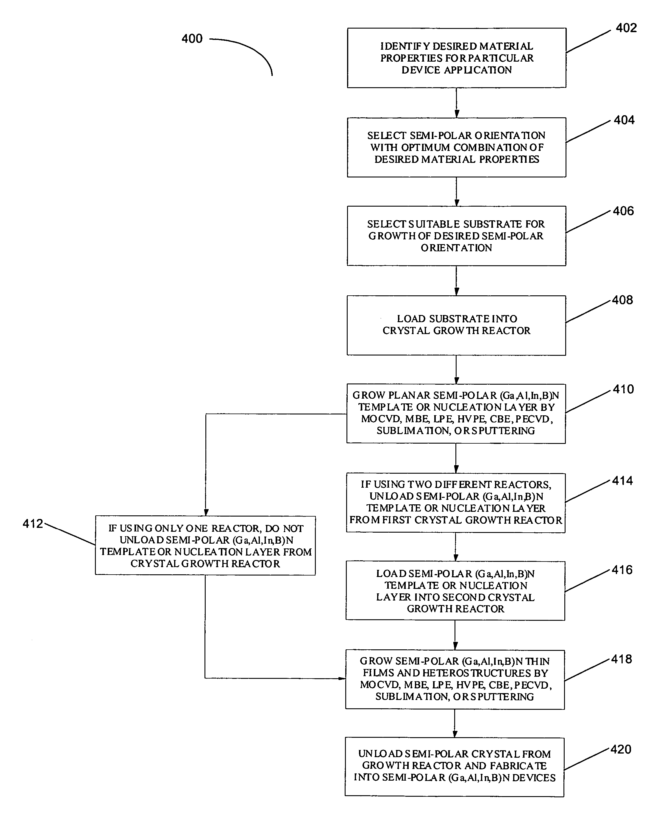
[0054] The present invention comprises a method for the growth and fabrication of semipolar (Ga,Al,In,B)N thin films, heterostructures, and devices. The flowchart 400 in FIG. 4 summarizes the salient steps for the growth of semipolar (Ga,Al,In,B)N thin films and heterostructures.
[0055] Steps 402 and 404 outline a top-down device design procedure used for selecting a semipolar growth orientation. First, the desired material properties (piezoelectric polarization, effective hole mass, etc.) for a particular device application need to be identified as shown in step 402. Based on th...
PUM
Abstract
A method for growth and fabrication of semipolar (Ga, Al, In, B)N thin films, heterostructures, and devices, comprising identifying desired material properties for a particular device application, selecting a semipolar growth orientation based on the desired material properties, selecting a suitable substrate for growth of the selected semipolar growth orientation, growing a planar semipolar (Ga, Al, In, B)N template or nucleation layer on the substrate, and growing the semipolar (Ga, Al, In, B)N thin films, heterostructures or devices on the planar semipolar (Ga, Al, In, B)N template or nucleation layer. The method results in a large area of the semipolar (Ga, Al, In, B)N thin films, heterostructures, and devices being parallel to the substrate surface.
Description
CROSS-REFERENCE TO RELATED APPLICATIONS [0001] This application claims benefit under 35 U.S.C § 119(e) of the following co-pending and commonly-assigned provisional application: [0002] Application Ser. No. 60 / 686,244, entitled “TECHNIQUE FOR THE GROWTH AND FABRICATION OF SEMIPOLAR (Ga,Al,In,B)N THIN FILMS, HETEROSTRUCTURES, AND DEVICES,” filed on Jun. 1, 2005, by Robert M. Farrell, Troy J. Baker, Arpan Chakraborty, Benjamin A. Haskell, P. Morgan Pattison, Rajat Sharma, Umesh K. Mishra, Steven P. DenBaars, James S. Speck, and Shuji Nakamura, attorneys docket number 30794.140-US-P1 (2005-668), which application is incorporated by reference herein. [0003] This application is also related to the following co-pending and commonly-assigned applications: [0004] U.S. Utility patent application Ser. No. 10 / 413,690, filed on Apr. 15, 2003, by Michael D. Craven, Stacia Keller, Steven P. DenBaars, Tal Margalith, James S. Speck, Shuji Nakamura, and Umesh K. Mishra, entitled “NON-POLAR (Al,B,In,G...
Claims
Application Information
Patent Timeline
Application Date:The date an application was filed.
Publication Date:The date a patent or application was officially published.
First Publication Date:The earliest publication date of a patent with the same application number.
Issue Date:Publication date of the patent grant document.
PCT Entry Date:The Entry date of PCT National Phase.
Estimated Expiry Date:The statutory expiry date of a patent right according to the Patent Law, and it is the longest term of protection that the patent right can achieve without the termination of the patent right due to other reasons(Term extension factor has been taken into account ).
Invalid Date:Actual expiry date is based on effective date or publication date of legal transaction data of invalid patent.
Inventor FARRELL, ROBERT M. JR.BAKER, TROY J.CHAKRABORTY, ARPANHASKELL, BENJAMIN A.PATTISON, P. MORGANSHARMA, RAJATMISHRA, UMESH KUMARDENBAARS, STEVEN P.SPECK, JAMES S.NAKAMURA, SHUJI